
Developing a commercial, production-ready IoT device is a multi-disciplinary engineering endeavor spanning electrical schematic design, multi-layer high-speed PCB layout, low-level embedded firmware, industrial RF compliance, and scalable mass manufacturing.
While software proofs-of-concept and hobbyist development kits (such as Arduino or Raspberry Pi) are useful for rapid benchtop demonstrations, deploying commercial B2B IoT devices into real-world factories, municipal utilities, smart agriculture fields, and logistics assets requires hardware built to survive relentless physical, electrical, and environmental stress.
This authoritative technical guide outlines the critical distinctions between lab prototypes and production B2B hardware, analyzes the 4 core subsystems of an IoT device, walks through DeviceLab's proven 6-stage development lifecycle, compares In-House development against partnering with an ODM/OEM engineering partner, and presents DeviceLab's turnkey IoT hardware engineering capabilities.
How Commercial B2B IoT Devices Differ from Lab Prototypes
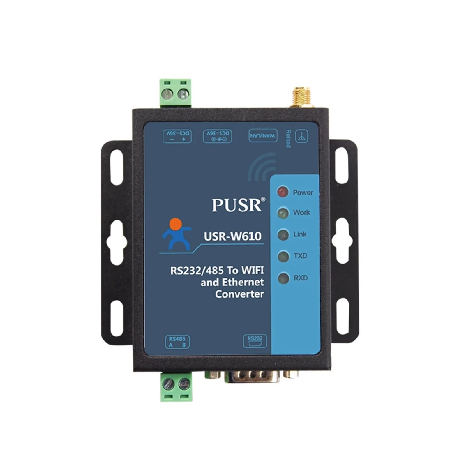
Many commercial IoT ventures stall during the transition from working lab prototypes to mass production. Benchtop prototypes are designed to validate functional software algorithms under ideal indoor conditions, whereas commercial B2B IoT devices must operate reliably in hostile physical environments without maintenance for years.
| Technical Criteria | Laboratory Prototype / DIY Setup | Commercial B2B IoT Production Device |
|---|---|---|
| Hardware Construction | Modular evaluation boards connected with loose Dupont jumper wires | Monolithic multi-layer PCBA (4–6 layers) using industrial SMT components |
| Power Management | Standard 5V DC power adapter via consumer USB connector | Industrial wide-input power (9–36V DC) or microamp-budgeted battery circuits |
| Environmental Protection | Bare circuit board or fragile 3D-printed enclosure | UL94-V0 flame-retardant plastic, IP65/IP67 waterproof and dustproof sealing |
| Electrical Circuit Hardening | No surge protection; vulnerable to reverse polarity and voltage spikes | Integrated PPTC resettable fuses, TVS surge diodes, and optical isolation |
| Hardware-Level Security | Plaintext flash storage, unprotected serial debug ports, default passwords | Hardware Secure Boot, AES-256 encrypted flash, and secure crypto elements |
| Lifecycle Maintenance | Manual firmware flashing requiring enclosure disassembly and physical cables | Automated remote Dual-Bank A/B FOTA updates with failsafe rollback |
| Compliance & Certification | Uncertified; unknown electromagnetic interference (EMI) characteristics | Engineered to meet CE, FCC, RoHS, and national telecommunications standards |
The Four Core Subsystems in IoT Device Engineering
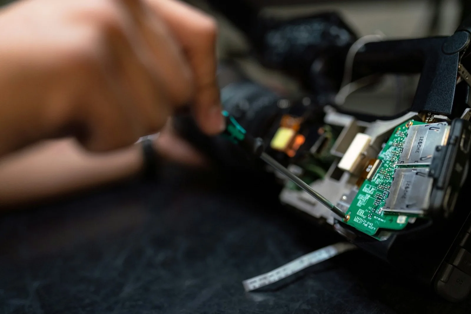
Every commercial IoT device comprises four interdependent hardware and software subsystems that must be designed to work in complete harmony:
CORE ARCHITECTURAL SUBSYSTEMS OF A COMMERCIAL IOT DEVICE:
┌────────────────────────────────────────────────────────┐
│  1. SENSING & ACTUATION SUBSYSTEM                      │
│  - Precision Analog Front-Ends (4-20mA, 0-10V, RTD)    │
│  - Digital Industrial Buses (RS485 Modbus, CAN, I2C)   │
├────────────────────────────────────────────────────────┤
│  2. CORE PROCESSING & SECURITY SUBSYSTEM               │
│  - Low-Power MCU / High-Performance SoC (ARM, RISC-V)  │
│  - Hardware Cryptographic Co-Processor & Secure Boot   │
├────────────────────────────────────────────────────────┤
│  3. WIRELESS CONNECTIVITY & RF SUBSYSTEM               │
│  - Cellular (4G LTE Cat-1/NB-IoT), LoRaWAN, BLE, Wi-Fi │
│  - 50-Ohm Impedance-Matched RF Front-End & Antennas    │
├────────────────────────────────────────────────────────┤
│  4. POWER MANAGEMENT & ENERGY BUDGETING                │
│  - Wide-Input DC-DC Buck / Boost Power Architecture    │
│  - Ultra-Low-Leakage Battery Management Subsystem      │
└────────────────────────────────────────────────────────┘
1. Sensing & Interface Subsystem
The interface subsystem captures physical environmental phenomena and conditions signals for the processor. Depending on the operational mandate, this includes analog front-ends (AFE) for temperature thermocouples, strain gauges, pressure transducers, vibration accelerometers, or industrial digital transceivers interfacing with Modbus RS-485, CAN Bus, and optical encoders.
2. Core Processing & Security Subsystem
The processing core manages device intelligence, sensor data aggregation, digital filtering, and network protocol execution. Industrial IoT devices leverage 32-bit ARM Cortex-M or RISC-V microcontrollers running deterministic RTOS firmware. Crucially, this block integrates hardware cryptographic engines holding unique device private keys for mutual cloud authentication (mTLS).
3. Wireless Connectivity & RF Antenna Engineering
Selecting the optimal wireless transmission technology depends on data throughput, transmission distance, and power constraints:
- Cellular IoT (4G LTE Cat-1 / Cat-M1 / NB-IoT): Delivers nationwide coverage for mobile assets, logistics trackers, and remote utility monitors without requiring local gateway infrastructure.
- LoRaWAN: Delivers long-range wireless telemetry (5–15 km) with ultra-low power consumption, making it ideal for agricultural soil sensing, municipal water metering, and sprawling industrial facilities.
- Bluetooth Low Energy (BLE 5.x): Ideal for short-range local sensor networks, industrial worker safety tags, and seamless smartphone commissioning.
- Wi-Fi 6 / Industrial Ethernet: High-bandwidth connectivity for edge AI vision cameras, vibration spectrum monitors, and smart building automation gateways.
4. Power Management & Battery Budgeting
Power design dictates whether an IoT device operates seamlessly or fails prematurely in the field. For mains-powered equipment, switching regulators must tolerate 9–36V DC industrial supply fluctuations and survive 2kV line surges. For battery-powered field nodes, engineers calculate microampere (µA) energy budgets—leveraging low-leakage LDOs, optimized sleep profiles, and high-energy lithium chemistries (such as Li-SOCl2) to guarantee 5 to 10 years of autonomous battery operation.
Complete 6-Step Turnkey IoT Development Process at DeviceLab
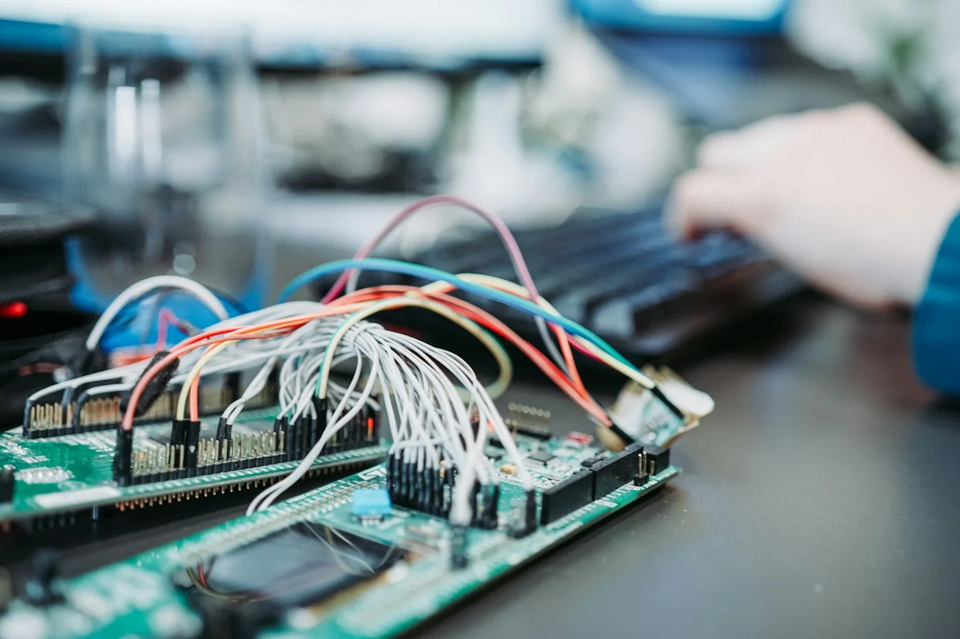
DeviceLab executes a disciplined 6-stage engineering roadmap designed to de-risk development, ensure regulatory compliance, and accelerate time-to-market:
DEVICELAB TURNKEY IOT R&D ROADMAP:
1. Field Feasibility Survey & Requirements Engineering (SRS & PRD)
      ↓
2. Hardware Architecture & Electrical Schematic Design
      ↓
3. Multi-Layer High-Speed PCB Layout & DFM/DFA Review
      ↓
4. Prototype Assembly, Bring-up & Functional Testing (Alpha Build)
      ↓
5. Harsh Field Pilot Trials & Pre-Compliance Certification (Beta Build)
      ↓
6. Production Tooling, Automated Testing Jigs & Mass Manufacturing
Step 1: Field Feasibility Survey and System Requirements Specification (SRS)
We work directly with your operational stakeholders to analyze on-site installation conditions, environmental hazards (temperature, humidity, explosive gases, electromagnetic noise), power availability, and network coverage. This results in an exhaustive System Requirements Specification (SRS) and Product Requirements Document (PRD).
Step 2: Electronic Hardware Schematic Design & BOM Optimization
DeviceLab engineers design complete electrical schematics, select tier-one industrial semiconductor components with guaranteed 10+ year availability, verify power delivery networks, and optimize the initial Bill of Materials (BOM) to hit target manufacturing cost targets.
Step 3: Multi-layer High-Speed PCB Layout & DFM/DFA Engineering
We execute multi-layer PCB layout (4 to 8 layers) adhering to strict Design for Manufacturing (DFM) and Design for Assembly (DFA) rules. This includes controlled-impedance RF trace routing, thermal relief dissipation, ground plane shielding, and high-voltage isolation creepage distances.
Step 4: Prototype Assembly, Bring-up & Functional Testing (Alpha Build)
Our rapid prototyping facility fabricates initial PCBA batches, mounts components via precision SMT pick-and-place, and conducts physical board bring-up. Firmware engineers load the initial Board Support Package (BSP), test peripheral communication buses with digital oscilloscopes, and validate base functionality.
Step 5: Harsh Environmental Field Pilot Trials & Pre-Compliance Certification (Beta Build)
Fully enclosed Beta units are deployed into real customer operating environments for extended pilot validation. Concurrently, devices undergo pre-compliance screening in testing laboratories for electrostatic discharge (ESD), surge immunity, radiated emissions (EMC), and thermal cycling (-40°C to +85°C).
Step 6: Production Tooling, Automated Testing Jigs & Mass Manufacturing Handover
Upon design freeze, DeviceLab designs custom automated testing fixtures (ATE jigs) that flash production firmware, inject cryptographic keys, calibrate analog sensors, and verify RF wireless power in under 60 seconds per unit during factory assembly.
In-House Hardware Development vs. Strategic R&D Partnership
Enterprises evaluating IoT device development face the strategic decision of building an internal hardware team or collaborating with an established R&D partner:
| Decision Criteria | Building an In-House Hardware Team | Partnering with DeviceLab (ODM/OEM) |
|---|---|---|
| Initial Capital Outlay | Substantial: Hiring specialized hardware, RF, layout, and firmware engineers; investing millions in oscilloscopes, spectrum analyzers, and testing equipment | Optimized: Predictable milestone-based engineering contracts without fixed operational overhead or lab equipment investments |
| Time-to-Market | Extended: 12 to 18+ months due to recruiting timelines, team onboarding, and inevitable learning-curve design respins | Accelerated: 3 to 6 months from concept to field pilot by leveraging proven, pre-validated hardware building blocks |
| Supply Chain Leverage | Limited: Low initial purchasing volumes result in high component prices, long factory lead times, and counterfeit risks | Extensive: Direct access to authorized global semiconductor distributors and established tier-one manufacturing partners |
| Intellectual Property | Retained internally | 100% full ownership of manufacturing files, schematics, PCB gerbers, and source code transferred upon project completion |
Custom IoT Engineering & Production Capabilities at DeviceLab
DeviceLab provides end-to-end original design and manufacturing services tailored to mission-critical B2B applications:
- Turnkey Hardware Engineering: Multi-layer PCB design, low-power analog front-ends, high-speed digital buses, and certified RF antenna matching.
- Industrial Firmware & Cloud Integration: Deterministic FreeRTOS and Embedded Linux development, cellular/LoRaWAN communication stacks, and secure MQTT/TLS cloud integration (AWS IoT Core, Azure IoT Hub).
- Industrial Mechanical Packaging & Enclosures: Custom IP65/IP67/IP68 enclosures engineered for UV stability, high impact resistance (IK08/IK10), and injection mold tooling.
- Flexible Production Batch Volumes: Supporting both agile pilot production runs (100–1,000 units) and high-volume automated manufacturing (10,000–100,000+ units).
Frequently Asked Questions (FAQ)
What is an IoT device in the most practical sense?
An IoT (Internet of Things) device is an autonomous physical electronic product that integrates sensors to capture real-world data, an onboard computing processor to analyze telemetry, and a wireless communications module to transmit operational data securely to cloud platforms or central management servers without human intervention.
What is the typical development cost for a custom commercial IoT device?
Total R&D investment depends on circuit complexity, industrial I/O density, environmental certifications, and enclosure tooling requirements. DeviceLab delivers fixed-scope milestone contracts covering requirements engineering, schematic capture, multi-layer PCB layout, prototype fabrication, firmware development, and pilot field trials.
How long does it take to advance from initial concept to a working field prototype?
For standard IoT devices leveraging proven processor architectures, DeviceLab typically delivers functional Alpha prototypes within 8 to 12 weeks. Full commercialization—incorporating pilot field validation, environmental pre-compliance testing, and production tooling—is typically completed within 4 to 6 months.
Does DeviceLab accommodate low-volume production or only mass manufacturing?
DeviceLab supports the complete product growth journey. We manufacture low-volume pilot batches (from 50 to 500 units) for customer trials and market validation, and seamlessly scale up to mass production runs (tens of thousands of units) using automated SMT pick-and-place assembly and custom functional testing fixtures.
How long can battery-powered IoT devices operate in the field?
Depending on data reporting intervals and battery chemistry, battery-operated IoT nodes engineered by DeviceLab operate continuously for 3 to 10+ years. We achieve this by optimizing ultra-low-power sleep modes (sub-10µA), selecting high-density lithium thionyl chloride (Li-SOCl2) batteries, and minimizing RF transmission time-on-air.
What are the primary trade-offs between 4G LTE and LoRaWAN connectivity?
4G LTE (Cat-1 / NB-IoT) provides high data bandwidth, low latency, and universal carrier coverage without requiring local gateways, but incurs recurring monthly SIM data costs and higher peak power draw. LoRaWAN offers exceptional long-range transmission (up to 15 km) and multi-year battery life with zero SIM carrier fees, but operates with restricted data payloads (typically a few dozen bytes per packet).
Who owns the intellectual property and manufacturing files upon project completion?
The client retains 100% intellectual property ownership. Upon project handover and milestone completion, DeviceLab transfers all design assets—including electrical schematics, PCB CAD files, Gerber fabrication archives, Bill of Materials, firmware source code, and enclosure CAD models.
How does DeviceLab ensure IoT devices cannot be hacked or compromised remotely?
We implement multi-layered hardware and software security: disabling hardware debug ports (JTAG) in production, activating silicon-level Secure Boot to prevent unauthorized code execution, encrypting internal flash storage with AES-256, and provisioning individual hardware cryptographic private keys for mutual cloud authentication (mTLS).
Can an enterprise develop an IoT product if they lack an internal technical engineering team?
Yes. DeviceLab operates as your outsourced Chief Technology Officer (CTO) and dedicated engineering department. We translate your high-level business goals into rigorous engineering specifications, manage the entire development lifecycle, and deliver completed, certified, production-ready hardware products.
Do manufactured IoT devices require regulatory testing and certification?
Yes. Commercial electronic devices emitting wireless radio frequencies must comply with statutory telecommunications and safety regulations (such as CE for Europe, FCC for the United States, and national telecom standards). DeviceLab designs all hardware to pass EMC/RF requirements from day one and manages the formal laboratory certification testing process.
Conclusion
Developing a successful commercial IoT device requires harmonizing electrical engineering, RF precision, embedded firmware resilience, industrial mechanical packaging, and scalable manufacturing economics. Avoiding fragile maker-grade components and partnering with experienced hardware development professionals ensures your connected device delivers continuous operational uptime, protects proprietary corporate data, and achieves an optimal return on investment.
DeviceLab is the trusted hardware R&D and ODM partner for enterprises modernizing operations through custom IoT technology. Contact our engineering team today to review your project requirements and turn your IoT product concept into a market-defining commercial reality.
Ready to Transform Your IoT Vision into a Commercial Reality?
Whether you require a compact cellular asset tracker, a LoRaWAN agricultural telemetry node, or an industrial RS-485 automation gateway, DeviceLab provides the end-to-end engineering excellence necessary to bring your product to market.
Contact our engineering specialists today for a detailed technical consultation, architecture review, and development proposal.
Engineering Guides & Satellite Articles Directory in Custom IoT Device Design & OEM/ODM Manufacturing
Complete technical documentation, wiring schematics, and field implementation guides in this cluster:
- The B2B Electronic Hardware Design Process: From Concept to Mass Production
- Industrial IoT Hardware: COTS vs. Custom Design Decision Framework
- IoT Proof of Concept to Hardware Prototype: Engineering Gateways & Transition Guide
- BOM Cost Optimization for B2B Electronics: Trimming 30% Without Compromising Quality
- Electronic Circuit & PCB Design Company in Hanoi: Hardware R&D Partner for B2B Enterprises
- What Determines PCB Design Costs? 2026 Hardware R&D Budget Estimation Guide
- Vietnam Hardware R&D Partner Guide: Engineering Capabilities, IP Protection & Rapid Prototyping
- IoT Device Manufacturer in Vietnam: Full Turnkey OEM/ODM Development from PoC to Mass Production