The total engineering cost to design a complete electronic circuit board (from initial schematics to an operational physical prototype) in Vietnam in 2026 typically spans from 12,000,000 VNĐ for basic control boards to approximately 50,000,000 VNĐ for multi-layer industrial microprocessor platforms or complex smart IoT gateways. Understanding this phased cost breakdown empowers project directors, startup founders, and chief engineers to budget their hardware R&D capital accurately, maintain financial control, and prevent unexpected scope creep.
This technical guide is part of DeviceLab's comprehensive engineering handbook on custom IoT device design and engineering.
📌 4 Core Drivers of Circuit Board Engineering Costs (Key Takeaways):
- Layer Stackup Complexity: 2-layer boards incur the lowest baseline layout costs (~3 - 6 million VNĐ; turnkey package from 12 million VNĐ); standard industrial 4-layer boards range from 6 - 12 million VNĐ layout fee; high-density 6-layer boards with high-speed processors range from 12 - 18 million VNĐ layout fee (with total turnkey prototype development reaching 45 - 50 million VNĐ).
- Component Density & Package Classes: Boards utilizing through-hole (DIP) or standard SMD passives (0805, 0603) route rapidly; assemblies featuring fine-pitch Ball Grid Array (BGA), leadless QFNs, or 0201 micro-passives require senior layout engineers to manage controlled impedance routing.
- Environmental Hardening Tier (Industrial vs. Consumer): Consumer electronics omit galvanic isolation; industrial designs mandate 2.5kV isolation barriers, flyback transformers, and TVS surge suppression, expanding simulation hours and BOM costs.
- International Regulatory Certification (CE, FCC, RoHS): Products destined for US/EU export require layout compliance with strict keep-out zones and dedicated pre-compliance test pads.
📊 Turnkey R&D Budget Framework by Project Tier (12 – 50 Million VNĐ):
- Tier 1 — Basic Control Circuit (2 Layers): 12,000,000 – 18,000,000 VNĐ. Step-down power rails, discrete sensor inputs, relay drivers, and basic 8-bit or 32-bit MCU for Proof-of-Concept testing or simple automation.
- Tier 2 — Connected IoT Device / Wearable (4 Layers): 18,000,000 – 32,000,000 VNĐ. Incorporates ESP32/STM32 MCUs, wireless transceivers (Wi-Fi, Bluetooth BLE, LoRa, 4G LTE), lithium battery charge management, and onboard RF trace antennas.
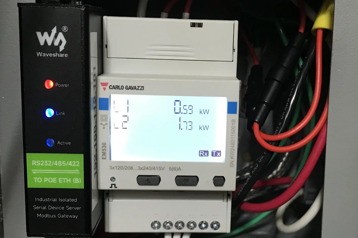
- Tier 3 — Industrial Edge Controller / Isolated Gateway (4 – 6 Layers): 32,000,000 – 50,000,000 VNĐ. Engineered for severe industrial noise environments: isolated RS485/Modbus, CAN Bus, Ethernet, high-energy TVS surge protection, and wide 9–36V DC industrial power rails.
2026 Itemized Prototype R&D Cost Breakdown Table
Below is a standardized engineering budget for a representative 4-layer industrial IoT gateway project (STM32/ESP32, 4G LTE modem, isolated RS485, and battery backup):
| No. | R&D Milestone Item | Detailed Engineering Deliverables | Price Range (VNĐ) |
|---|---|---|---|
| 1 | Schematic Circuit Design | Component selection, Buck/Boost power stages, MCU architecture, isolated RS485 interface, and battery BMS. Delivers SchDoc and PDF schematics. | 4,000,000 - 6,500,000 |
| 2 | PCB Multi-Layer Layout Routing | 4-layer DFM routing, 50-ohm RF impedance matching for 4G antenna, EMI noise containment. Delivers Gerber, Drill, and CPL Pick & Place files. | 6,000,000 - 10,500,000 |
| 3 | Bare PCB Sample Fabrication | Fabrication of 5 prototype bare boards in FR4 TG150 with ENIG gold plating and 100% Flying Probe electrical testing. | 1,200,000 - 2,200,000 |
| 4 | BOM Sourcing & Laser Stencil | High-precision frameless laser stencil + complete genuine component kit for 5 prototypes sourced via Mouser/DigiKey/LCSC. | 3,500,000 - 6,500,000 |
| 5 | Automated SMT Assembly & AOI | Pick-and-place machine run, multi-zone reflow oven soldering along certified thermal profiles, and 100% Automated Optical Inspection (AOI). | 1,800,000 - 3,300,000 |
| 6 | Firmware Bring-Up & Validation | Diagnostic test firmware exercising all hardware peripherals (GPIO, UART, I2C, SPI, Flash, 4G, ADC), calibration, and 72-hour burn-in stress test. | 5,500,000 - 9,000,000 |
| TOTAL TURNKEY INVESTMENT FOR FULLY FUNCTIONAL PROTOTYPE | 22,000,000 - 38,000,000 VNĐ | ||
* Note: The table above reflects a standard 4-layer IoT Gateway prototype. For simpler 2-layer control boards, turnkey project budgets start from just 12,000,000 VNĐ. Complex industrial microprocessor systems requiring specialized peripheral routing and extensive certification testing range between 35,000,000 – 50,000,000 VNĐ.
How to Curtail Circuit Design Expenses Without Sacrificing Reliability
- 1. Freeze Product Scope Early (Prevent Scope Creep): The single largest driver of budget inflation is modifying peripheral interfaces midway through routing. Craft a rigorous Product Requirements Document (PRD) and lock specifications before layout kicks off.
- 2. Leverage Pre-Certified Wireless Modules: Rather than engineering discrete RF transceivers chip-down (costing thousands of dollars in anechoic chamber testing), utilize pre-certified modules such as the Quectel EC200 (for 4G) or ESP32-WROOM (for Wi-Fi/BLE) bearing established FCC/CE marks.
- 3. Standardize Board Outlines to Standard Panel Sizes: Designing boards that panelize efficiently within standard 100x100mm or 150x200mm fabrication panels saves significant FR4 copper laminate material waste.
Receive a Detailed Circuit Design Estimate Within 24 Hours
Submit your block diagrams or preliminary product concepts to DeviceLab. Our hardware engineering team will evaluate technical feasibility, suggest optimized BOM parts, and return an itemized budget estimate.
Technical Hotline: (+84) 982.503.355