Scaling an Internet of Things (IoT) hardware product from an initial proof-of-concept (PoC) breadboard into a reliable, certified, mass-manufactured device is an intricate journey fraught with supply chain hurdles, regulatory compliance traps, and manufacturing yield risks. For international tech enterprises and innovative startups seeking high-quality electronics manufacturing without excessive overheads, Vietnam has emerged as the premier turnkey Original Design & Equipment Manufacturing (ODM/OEM) destination in the Asia-Pacific region. This guide details the complete end-to-end production workflow—from DFM review to high-speed SMT assembly and automated test fixtures.
This technical guide is part of DeviceLab's comprehensive engineering handbook on custom IoT device design and engineering.
📌 Turnkey Production Architecture in Vietnam (Key Takeaways):
- Design for Manufacturing (DFM) Review: Comprehensive audits of component clearances, thermal dissipation relief, and fiducial markings before launching production stencils, guaranteeing >99% SMT first-pass yield.
- Automated Test Equipment (ATE) Jigs: Custom-engineered bed-of-nails test fixtures running automated Python/C test routines that verify 100% of power rails, RF transmission power, and sensor interfaces in under 45 seconds per board.
- Flexible Batch Economics: High-mix production capabilities supporting pilot runs from 100 to 500 units, scaling seamlessly up to batch volumes of 5,000 to 50,000 units.
- Global Logistics & Compliance: Full assistance with international certification (FCC Part 15B, CE RED, RoHS, REACH) and bonded warehouse logistics for express global container dispatch.

The 5 Crucial Stages of Turnkey IoT Device Manufacturing
| END-TO-END TURNKEY PRODUCTION ROADMAP IN VIETNAM |
+-----------------------------------------------------------------------------------+
| STAGE 1: DFM/DFT Engineering Audit & Authorized Component Sourcing (BOM Scrub) |
| |
| STAGE 2: Engineering Verification Test (EVT) - 5 to 20 Prototype Units |
| |
| STAGE 3: Design Verification Test (DVT) - Tooling, Enclosure Mold & Pre-Compliance|
| |
| STAGE 4: Production Verification Test (PVT) - Pilot Run (100 - 500 Units) with ATE|
| |
| STAGE 5: Mass Production (MP) - High-Volume SMT, Conformal Coating & Global Export|
+-----------------------------------------------------------------------------------+
Stage 1: DFM / DFT Optimization and Global Component Sourcing
Before ordering bare PCBs or cutting stencils, our manufacturing engineers perform an extensive Design for Manufacturing (DFM) and Design for Testing (DFT) review. We scrutinize component spacing to prevent solder bridging, confirm thermal relief pad designs for wave soldering, and scrub the Bill of Materials (BOM) against authorized global distributors to mitigate counterfeit component risks and ensure long-term component availability.
Stage 2 & 3: EVT and DVT Validation
During the Engineering Verification Test (EVT), functional prototypes are assembled and subjected to rigorous bench testing: thermal cycling in environmental chambers, power consumption profiling across active/sleep modes, and RF antenna tuning. In parallel, custom plastic injection molds or extruded aluminum tooling are fabricated to produce production-grade mechanical enclosures.
Stage 4: PVT Pilot Run and Custom ATE Test Fixture Integration
To eliminate manual testing bottlenecks and human error on the factory floor, DeviceLab designs proprietary Automated Test Equipment (ATE) fixtures (commonly referred to as "Bed-of-Nails" test jigs). Pneumatic clamps press the assembled PCB against spring-loaded pogo pins contacting dedicated test points. In less than 45 seconds, the automated test software flashes production firmware, programs unique MAC addresses and cryptographic keys, measures all voltage rails, and verifies RF transmission power.
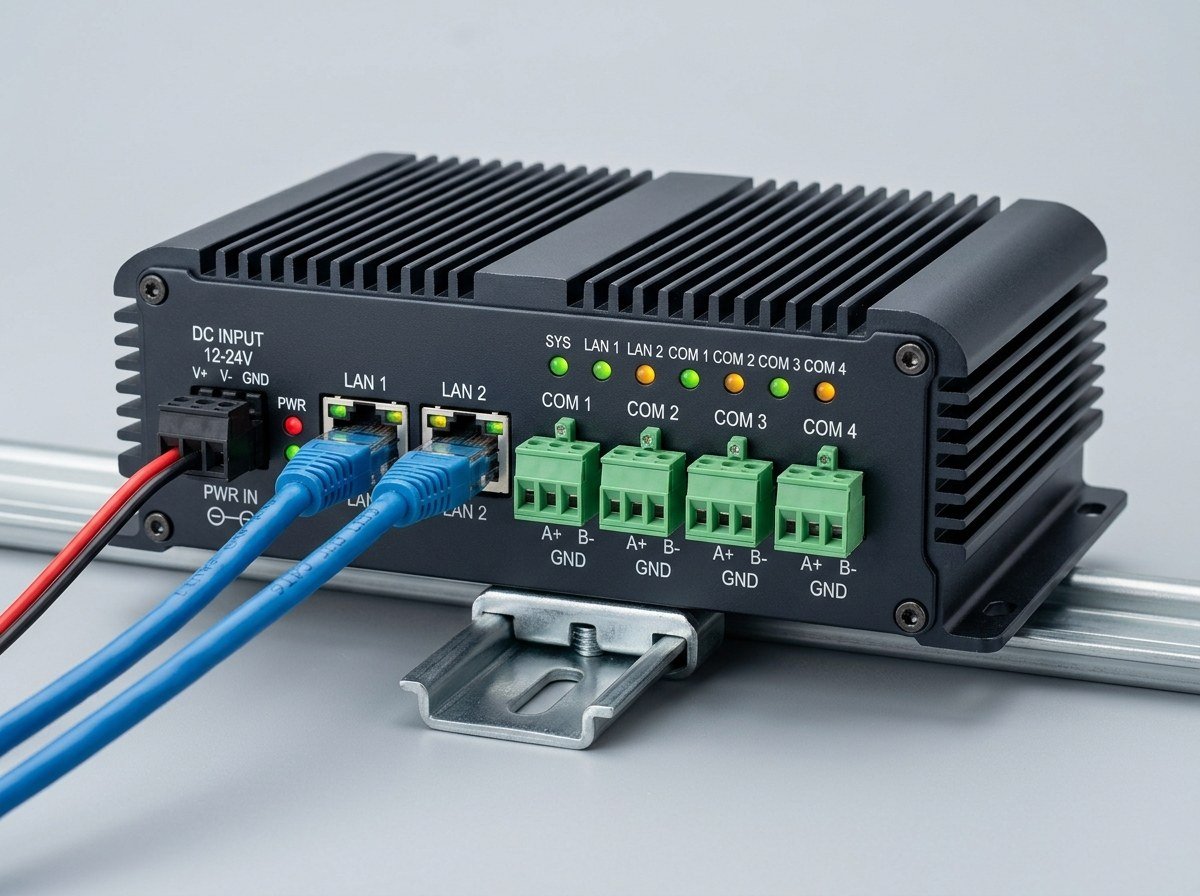
Quality Assurance Standards & Environmental Screening
Industrial IoT hardware demands superior reliability in harsh field environments. DeviceLab enforces rigorous quality control protocols across all manufacturing lines:
- Automated Optical Inspection (AOI): High-resolution multi-angle cameras inspect 100% of solder joints, identifying solder bridges, insufficient wetting, tombstoning, and component polarity errors.
- X-Ray Inspection (AXI): Essential for bottom-terminated components (QFN, BGA), confirming that solder voiding remains well below the IPC-A-610 Class 2 limit of 25%.
- Burn-In Screening Chambers: Devices run continuous loop diagnostics under elevated ambient temperatures (+60°C to +70°C) for 24 to 48 hours to weed out infant mortality defects.
- Protective Conformal Coating: Automated selective spray coating applying acrylic or silicone conformal coatings to safeguard delicate circuits against industrial humidity, chemical vapors, and dust ingress.
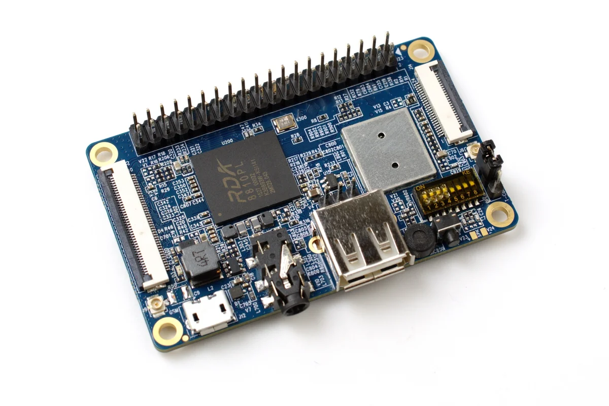
White-Label Branding, Packaging & Door-to-Door Logistics
DeviceLab provides comprehensive white-label OEM customization, enabling foreign brands to deliver finished, market-ready products directly to their end customers:
- Custom Laser Marking & Silk-Screening: Inscribing your brand logo, regulatory compliance marks (CE, FCC, UKCA), and unique QR/barcodes onto enclosures.
- Custom Industrial / Retail Packaging: Custom foam inserts, printed retail boxes, multi-lingual quick-start guides, and tamper-evident security seals.
- International Export Logistics: Coordinating export customs clearance from Noi Bai International Airport (HAN) or Hai Phong Seaport, with express air freight delivery (FedEx/DHL) or ocean container shipping directly to your fulfillment warehouse.
Request a Manufacturing Feasibility & BOM Cost Analysis
Send us your Gerber files and Bill of Materials (BOM). Our manufacturing team will evaluate production feasibility, calculate turnkey unit economics, and provide a competitive quotation within 3 business days.
Email: hi@devicelab.vn | WhatsApp: +84 982 503 355