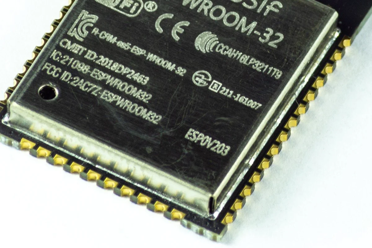
Custom electronic hardware development (Custom Electronic R&D) is the end-to-end engineering discipline of translating commercial product concepts into reliable, mass-producible electronic devices—spanning schematic design, multi-layer PCB layout, embedded firmware development, mechanical enclosure modeling, prototype validation, and regulatory compliance.
This technical guide is part of DeviceLab's comprehensive engineering handbook on custom IoT device design and engineering.
Many businesses in Vietnam attempt to commercialize electronic hardware by cobbling together hobbyist development boards (Arduino, Raspberry Pi, ESP32 breakout boards) inside 3D-printed enclosures. While adequate for early software validation, these makeshift assemblies invariably fail in commercial environments: unstable power rails, severe vulnerability to electrical noise, lack of industrial certifications (QCVN, CE, FCC), and components that cannot be reliably sourced for mass production.
This technical guide details DeviceLab's standardized 5-phase electronic R&D lifecycle, analyzes the critical technical milestones required to bring hardware to market, and exposes the three fatal pitfalls that derail hardware startups and engineering projects.
What is Custom Electronic Device Design?
Custom electronic hardware development is an integrated engineering process that delivers optimized, purpose-built circuit boards (PCBA) and enclosures tailored precisely to a product's functional, environmental, and commercial constraints.
Unlike off-the-shelf development kits, custom industrial hardware integrates power protection, specialized sensors, industrial bus transceivers, and secure embedded firmware directly onto a single unified board, driving down bill-of-materials (BOM) costs while maximizing physical durability.

Where Should Your Project Start?
Depending on your current technical assets, DeviceLab structures R&D workflows to match your exact entry point:
| Your Current Asset Status | Available Input Materials | Recommended R&D Trajectory | Delivered Engineering Output |
|---|---|---|---|
| Raw Commercial Idea | Written concept brief, target market specifications, competitor reference samples | Comprehensive PRD definition, component selection, proof-of-concept breadboarding | Complete System Architecture Specification & Bill of Materials (BOM) budget |
| Proof-of-Concept Prototype | Arduino / ESP32 breadboard demo, basic functional script | Industrial schematic capture, multi-layer PCB layout, DFM/EMC optimization | Industrial schematic files, Gerber layout packages, and PCBA prototype boards |
| Existing PCB Requires Redesign | Legacy Gerber files, BOM list, or physical circuit board sample | Reverse engineering, component obsolescence mitigation, cost reduction redesign | Modernized PCB layout, updated BOM with active supply chain availability |
| Ready for Mass Production | Validated Gerber files, CAD STEP files, and firmware source code | Mass production jig design, test firmware authoring, automated SMT assembly | Turnkey manufactured, tested, and boxed commercial hardware products |
5 Standardized R&D Phases in Electronic Product Development
Bringing a commercial electronic device from concept to high-volume manufacturing requires strict adherence to a gated engineering process:
Phase 1: Product Requirement Document (PRD) & System Architecture
The foundation of every successful hardware project. The engineering team collaborates with the client to define: * Operating environment: operating temperature (-20°C to +70°C), ingress protection (IP65/IP67), vibration resistance. * Power architecture: AC mains, 24VDC industrial bus, battery operation, or PoE; peak current budgets and sleep-mode quiescent current limits. * Communication interfaces: RS485, CAN bus, 4G LTE, Wi-Fi, BLE, LoRa, or Ethernet. * Target unit manufacturing cost (COGS / Target BOM) and regulatory requirements (QCVN, CE, FCC).
Phase 2: Schematic Design & Multi-Layer PCB Layout
Hardware engineers select silicon components with guaranteed manufacturer lifecycle availability (>7–10 years). Schematics are captured with multi-stage ESD protection, reverse-polarity diodes, and decoupling networks. The PCB is laid out on 4 to 8 layers with dedicated ground planes, impedance-controlled trace routing, and strict Design for Manufacturing (DFM) rules.
Phase 3: Embedded Firmware Development & System Integration
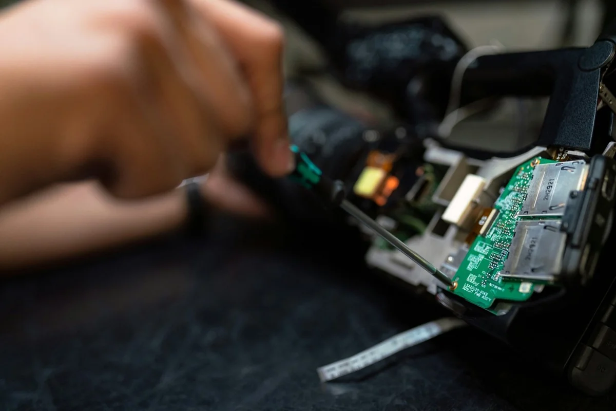
Firmware is authored in C/C++ on top of real-time operating systems (FreeRTOS or Zephyr) or Embedded Linux. Core engineering focuses on: * Multi-stage Hardware Watchdog timers to guarantee self-healing from unexpected lockups. * Non-volatile Flash storage with wear-leveling algorithms. * Secure dual-bank Fail-safe Firmware Over-The-Air (FOTA) update mechanisms. * Cryptographic authentication and encrypted communication pipelines (TLS 1.3, AES-256).
Phase 4: 3D Mechanical Enclosure Engineering & Thermal Simulation
Industrial mechanical engineers develop 3D CAD models (STEP format) matching the PCB assembly. The enclosure is designed for injection-molded ABS/polycarbonate or CNC-machined anodized aluminum, incorporating silicone sealing gaskets, thermal dissipation paths, and standard DIN-rail or wall mounting brackets.
Phase 5: Prototype Fabrication & Laboratory Validation
First-article prototypes (5–10 units) are assembled via SMT lines and subjected to rigorous laboratory screening: * Signal integrity verification via high-bandwidth digital oscilloscopes. * Thermal imaging under 100% full-load operation inside thermal chambers. * Accelerated life testing (ALT) and continuous 72-hour operational burn-in. * Pre-compliance EMC screening (ESD, Surge, EFT) to guarantee certification success.
3 Fatal Mistakes That Derail Electronic Hardware Projects
- Selecting Gray-Market or Sole-Source Components: Designing a product around specialized ICs with single distributors leads to project failure when global supply chains tighten or component lead times stretch past 52 weeks. DeviceLab mandates multi-sourcing and pin-compatible second-source components for all critical silicon.
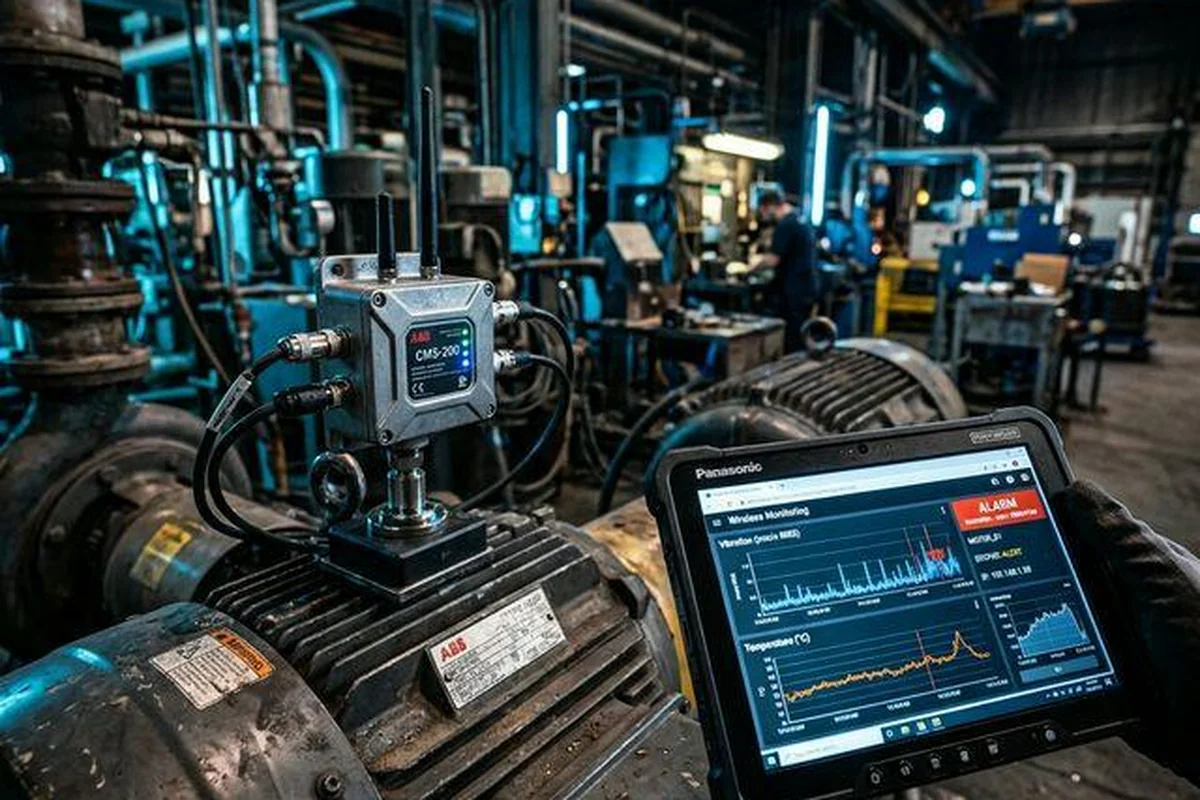
- Overlooking Thermal Dissipation & Ingress Protection: Devices that operate reliably on an air-conditioned laboratory bench frequently overheat or reset when installed inside enclosed industrial cabinets at 60°C ambient temperatures.
- Postponing Regulatory Compliance to the Final Stage: Failing to design for EMC/EMI compliance from the initial PCB layout stage forces costly, time-consuming schematic and PCB respins when devices fail statutory certification tests.
DeviceLab Hardware R&D Engineering Commitments
DeviceLab provides end-to-end electronic hardware R&D with clear engineering deliverables: * 100% IP & Design Ownership: Clients retain complete ownership of all schematic files (Altium/KiCad), Gerber packages, BOM lists, CAD STEP files, and firmware source code. * Industrial Reliability Guarantee: All designs strictly adhere to IPC-A-610 Class 2/3 manufacturing standards and pass rigorous environmental stress testing. * Seamless Production Transition: In-house SMT prototyping lines bridge the gap between initial prototypes and high-volume mass production without design transfer friction.
Frequently Asked Questions (FAQ)
1. Can I hire DeviceLab to develop a product if I do not have a schematic diagram?
Absolutely. Over 70% of our clients begin with only a commercial functional specification or a basic concept document. DeviceLab formulates the comprehensive PRD, selects optimal components, captures schematics, and executes layout from scratch.
2. How long does it take to develop a functional commercial prototype?
Depending on device complexity, typical engineering timelines average 4 to 8 weeks: 2–3 weeks for schematic capture and multi-layer layout, 1–2 weeks for PCB fabrication and SMT assembly, and 1–3 weeks for firmware integration and laboratory burn-in.
3. What cost components make up a turnkey electronic R&D project?
Project costs comprise three primary elements: Non-Recurring Engineering (NRE) fees for schematic/layout/firmware design, physical prototype fabrication expenses (PCB fabrication, components, SMT stencils, 3D printing/CNC tooling), and optional regulatory certification testing fees.
4. Does DeviceLab handle mass manufacturing after R&D is complete?
Yes. We provide turnkey manufacturing services—from pilot batches (100–500 units) to full mass production (10,000+ units)—encompassing component procurement, automated SMT/THT assembly, conformal coating, automated functional testing (FCT), and final retail packaging.
5. Are components sourced domestically in Vietnam or imported?
Critical active silicon (MCUs, RF transceivers, power management PMICs) is sourced directly through franchised global distributors (Digi-Key, Mouser, Arrow, Element14) with full manufacturer traceability (CoC), while passive components and mechanical enclosures are sourced efficiently through vetted regional manufacturing partners.
6. Does the client retain full ownership of the firmware source code?
Yes, 100%. Upon final milestone sign-off, all firmware repositories (C/C++ source code, build scripts, libraries) and hardware design files are transferred to the client with full commercial usage rights.
7. Does DeviceLab support statutory product certification testing?
Yes. We perform pre-compliance EMC and RF testing in our internal lab to verify performance before accompanying client devices through accredited testing laboratories for official QCVN, CE, or FCC certification.
Transform Your Idea into a Commercial Hardware Product
If your enterprise is preparing to engineer a custom IoT device, industrial controller, or proprietary electronic product:
👉 Submit Your PRD & Schedule a Technical Consultation
Or consult directly with DeviceLab's Chief Hardware Architect via Hotline/WhatsApp/Zalo: 0982.503.355 to receive an engineering feasibility review and project cost estimate.