Skip to content

Engineering Partner · Hardware R&D & Embedded Systems

Why Leading Enterprises Partner with DeviceLab

Far beyond basic PCB drafting or reselling boxed gadgets. We co-engineer your hardware systems from concept through scalable volume production.

Electronic hardware engineering is unforgiving. In technology, there is an enduring truth: “Hardware is hard.” While software bugs can be patched in minutes, a miscalculated power architecture, an under-resourced microcontroller, or neglected thermal dissipation inside an industrial switchgear panel can cost tens of thousands of dollars and months of lost market momentum.

DeviceLab operates as your dedicated Engineering Partner: we dissect your operational challenges, recommend the lowest-risk architecture, and stand beside you across physical hardware, low-level firmware, and cloud networking until your product operates reliably in the field.

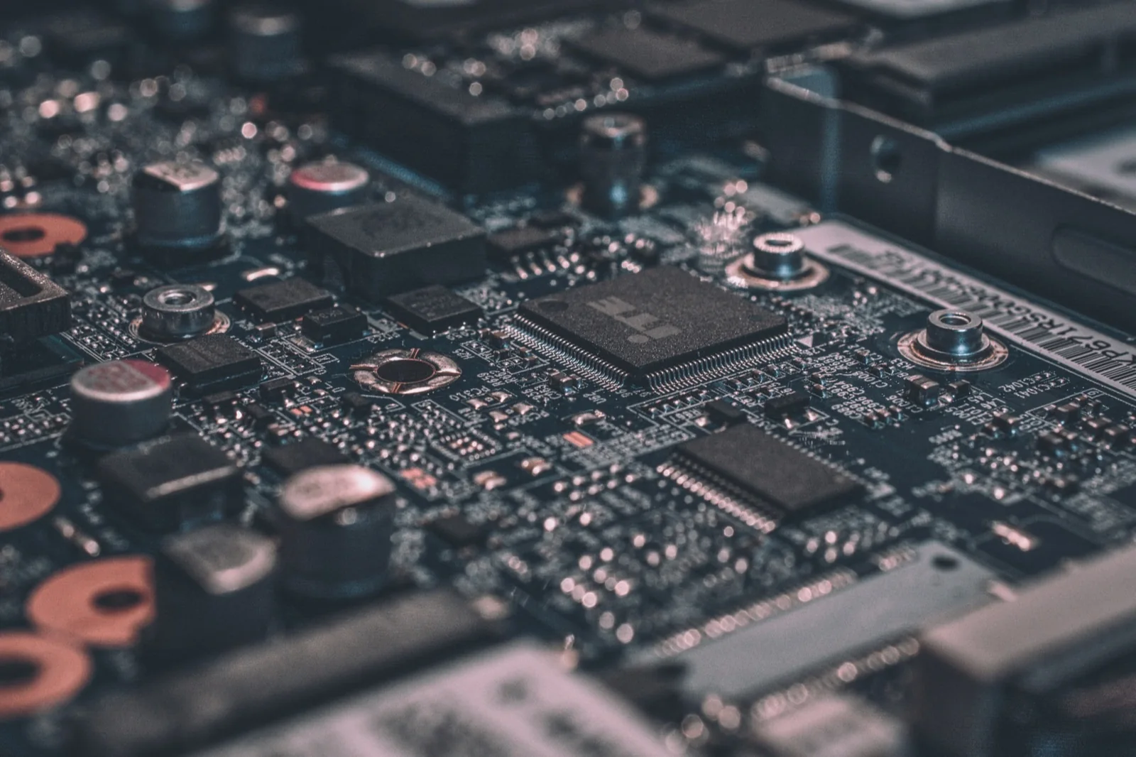
DeviceLab senior engineers analyzing signal waveforms and power rails on real test bench hardware

Core Value: 5 Reasons Enterprises Choose DeviceLab

  • 1. Problem-First Engineering Philosophy: We never push for unnecessary custom PCB redesigns if your problem can be solved faster and more cost-effectively using proven COTS equipment or customized OEM/SOM platforms.
  • 2. Single-Source Full-Stack Mastery: Seamless execution across Hardware (Schematics & Multi-layer PCB) + Embedded Firmware + Networking Protocols + Edge AI & Cloud Backends. Zero finger-pointing between vendors.
  • 3. Engineered to Survive Harsh Field Realities: Wide-temperature industrial components (-40°C to +85°C), optical galvanic isolation, high-energy TVS surge protection, and autonomous Local-First operation.
  • 4. Designed for Commercial Volume (DFM): Rigorous BOM cost modeling, component lifecycle de-risking, second-sourcing, and automated SMT factory test fixtures (FCT Jigs).
  • 5. 100% Intellectual Property Ownership: You retain complete, unencumbered ownership of Altium schematics, Gerber files, production BOMs, and uncompiled firmware source code under robust NDA protection.

Resource Reality Check

Building an In-House Hardware Team vs. Partnering with DeviceLab

Founders and CTOs frequently evaluate whether to hire an internal hardware team or partner with a specialized engineering house. Here is the objective 12-month balance sheet.

Evaluation Criteria Building an In-House Hardware Team Co-Engineering with DeviceLab
Engineering Headcount Requires at least 3–4 senior hires: 1 Hardware PCB engineer, 1 Embedded Firmware specialist, 1 Mechanical engineer, and 1 Engineering Lead. Immediate access to an established, cross-disciplinary team without recruitment overhead or equity dilution.
Monthly Fixed Burn Rate $8,000 – $15,000+ per month in salaries, benefits, facility overhead, and EDA software licenses (Altium / SolidWorks). Milestone-based, fixed-scope proposals tied directly to deliverables. Zero recurring payroll liability.
Lab Equipment & Test Instrumentation Requires $25,000 – $50,000 in capital expense: digital storage oscilloscopes, logic analyzers, precision DC supplies, RF spectrum analyzers, and rework stations. 100% utilization of DeviceLab’s established hardware laboratory, load test benches, and instrumentation.
Time-to-Market Kickoff Takes 2–4 months to recruit, onboard, and establish workflows before designing a single schematic line. R&D kickoff and architectural block diagram formulation begins within week one post-NDA execution.
Field Failure Pitfalls Prone to painful learning curves: ground loops, EMI radiation failures, memory leaks, and obsolete component selections (EOL). Directly leverages proven circuit blocks and firmware frameworks validated across tens of thousands of active field hours.
Personnel Attrition Risk A key engineer departing mid-project can freeze development, scatter undocumented source code, and force a restart. Corporate legal contract with standardized documentation, structured Git repositories, and institutional continuity.

DeviceLab does not displace your product vision. We serve as your high-velocity engineering arm—bringing your hardware products to market faster, with minimized technical risk and controlled capital expense.

Who We Serve

Ideal Partner Profiles for DeviceLab

Every client engaging DeviceLab faces distinct engineering bottlenecks. We listen carefully to deliver targeted technical solutions.

1. Tech Startups & Product Innovators

The Bottleneck: You have a breakthrough product concept or an early Arduino/Raspberry Pi bench demo, but lack the multidisciplinary engineering bench to productize it into a commercial, certification-ready device. You fear wasting capital on generic drafting services that deliver unviable boards.

How DeviceLab Helps: We work directly from functional briefs (no schematics needed), evaluate COTS vs. Custom development, build industrial-grade prototypes, and model target unit BOM economics so you can pitch investors and early enterprise customers with absolute confidence.

2. Industrial Manufacturing & Plant Operations

The Bottleneck: You must extract telemetry from legacy machines (Modbus RS485, Siemens/Mitsubishi PLCs) or monitor facility power sub-meters. Standard market gadgets don’t fit your switchgear cabinet, speak proprietary protocols, or crash due to severe industrial harmonics.

How DeviceLab Helps: We conduct on-site electrical surveys and engineer rugged Industrial IoT Gateways equipped with optical isolation and surge suppression—streaming field telemetry safely to SCADA/MES dashboards without disrupting active production lines.

3. System Integrators (SI) & Infrastructure Contractors

The Bottleneck: Deploying industrial telemetry, machine monitoring, or vision AI inspection systems for manufacturing and infrastructure. Foreign commercial brands are exorbitant, require 3–6 month lead times, and refuse to customize operational software for regional workflows.

How DeviceLab Helps: We provide turnkey OEM/ODM hardware platforms (such as Industrial IoT Gateways and Edge AI Boxes), delivering domestic supply chain availability, rapid lead times, and tailored firmware customization.

4. Software & Cloud SaaS Engineering Teams

The Bottleneck: Your engineering team excels at Cloud infrastructure, Web apps, and mobile UX, but hits a wall when connecting to physical devices: boards drop offline, firmware locks up requiring hard power cycling, or no safe dual-bank OTA pipeline exists.

How DeviceLab Helps: We bridge the physical gap: capturing custom hardware, writing deterministic firmware, and serializing telemetry into clean, predictable MQTT/JSON or RESTful schemas with hardware watchdog recovery.

Honest Engineering Philosophy

We Never Force a Custom Board If You Don’t Need One

A widespread misconception in hardware development is that every product requires a ground-up PCB from day one. We objectively evaluate 3 execution paths to protect your budget.

  1. 1. Commercial Off-The-Shelf (COTS)
  2. 2. Platform Customization (OEM / SOM)
  3. 3. Full Custom Development

How do we determine the right path? The decision hinges on 5 core parameters: Functional specifications, Time-to-market urgency, Upfront NRE budget, Mechanical form factor constraints, and Forecasted annual volume.

  • COTS Integration (Off-The-Shelf): Harnesses certified, commercially available industrial hardware. Best for standard telemetry deployments requiring commissioning in 1–2 weeks.
  • OEM / SOM Customization (Platform-based): Leverages proven System-on-Modules (Compute Modules / SOMs), designing only custom carrier boards and specialized firmware. Cuts R&D timeline and NRE expenditure by 50%.
  • Full Custom Development (Ground-Up): Schematic capture, multi-layer PCB layout, and discrete silicon component selection. Mandatory when products require ultra-slim mechanical envelopes, multi-year battery operation, or high production volumes to minimize unit BOM cost.

If an off-the-shelf solution solves your challenge, we will advise you to use it. We only propose custom hardware when it delivers a decisive competitive or economic advantage.

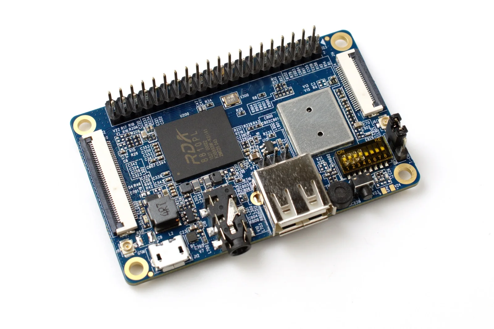
Industrial compute modules and SOM platforms leveraged for rapid OEM/ODM customization

Unified Competency

Full-Stack Technological Mastery: Zero Finger-Pointing

A commercial hardware device only succeeds when schematics, firmware, networking protocols, and cloud platforms operate in perfect harmony.

  • System Architecture Design
  • Schematic & Multi-Layer PCB Layout
  • Embedded C/C++ Firmware
  • Embedded Linux BSP & RTOS
  • Industrial Fieldbus & Wireless RF
  • Edge AI & Computer Vision
  • Cloud Platform & Web Dashboards
  • Mechanical Enclosure CAD & DFM

One of the most frustrating experiences in hardware development is vendor finger-pointing: The PCB designer blames the firmware developer, the firmware developer claims the hardware lacks adequate power rail decoupling, and the cloud software team insists the device sends corrupted payloads. The project derails for months while nobody assumes responsibility.

At DeviceLab, we assume unified responsibility across the complete technology chain. When an anomaly occurs—whether a power surge transient, a microsecond interrupt race condition, or a packet synchronization delay—our engineers troubleshoot it directly on the lab bench until the root cause is resolved.

Hardware system validation on test benches inside the DeviceLab engineering laboratory

Harsh-Environment Engineering

Engineered to Survive and Excel in Unforgiving Realities

A prototype board operating on an air-conditioned desk at 25°C provides zero assurance that it will survive 5 years inside a sealed 55°C industrial cabinet bombarded by conductive metal dust and mechanical vibration.

To ensure 24/7/365 uninterrupted autonomous operation without requiring manual field resets, DeviceLab enforces rigorous industrial design standards:

  • Local-First Autonomous Architecture: Edge hardware makes local decisions and caches data autonomously. If an internet link or cloud server goes offline, local control and telemetry logging continue uninterrupted; once restored, cached records seamlessly reconcile.
  • Galvanic Isolation & Surge Suppression: TVS high-voltage clamp diodes, common-mode EMI chokes, and optical galvanic isolation protect all RS485, CAN, and Ethernet communication interfaces against lightning surges and ground loops.
  • Independent Hardware Watchdog: Dedicated external supervisor ICs continuously monitor microcontroller state, cleanly power-cycling systems upon transient firmware lockups.
  • Conformal Coating & Environmental Sealing: Protective conformal coatings shield PCB surfaces against tropical humidity and airborne contaminants, paired with passive thermal dissipation enclosures.
Industrial-grade PCBA featuring comprehensive power protection and high-immunity filtering

From Lab to Factory Floor

Engineering for Mass Production, Not Just One-Off Bench Prototypes

Assembling a single working prototype represents only 30% of the journey. The remaining 70% is engineering the board so that 1,000 or 10,000 units can be produced with high manufacturing yield, low defect rates, and predictable unit economics.

From initial schematic capture, DeviceLab engineers for volume reality:

  • Supply Chain Lifecycle De-risking: Strict avoidance of End-Of-Life (EOL) or Not Recommended For New Designs (NRFND) silicon. Pin-compatible second-source components are engineered into the layout to prevent production halts during component allocations.
  • Design for Manufacturing (DFM/DFA): Component clearances, thermal relief pads, and automated test points (ICT/FCT) are calibrated for high-speed automated SMT pick-and-place and Automated Optical Inspection (AOI).
  • Automated Functional Test Fixtures (FCT Jigs): We design custom pogo-pin test jigs enabling factory technicians to flash firmware, calibrate analog rails, and run comprehensive go/no-go functional validation in under 30 seconds per board.

We ensure your product transitions to volume manufacturing seamlessly—with zero costly production surprises.

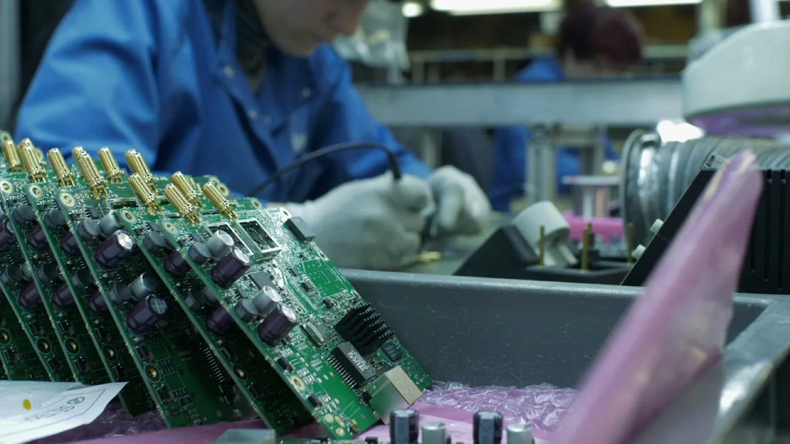
Quality control inspection and automated test fixtures on electronic assembly production lines

Clarity & Integrity

Projects DeviceLab Declines to Undertake

To ensure mutual respect and eliminate mismatched expectations, we are transparent regarding assignments DeviceLab does not accept:

No Academic Assignments or Hobbyist Kits

We are a professional engineering R&D firm focused exclusively on commercial hardware and industrial deployments. We do not accept university graduation theses, academic homework, or hobbyist tinkering without commercialization intent.

No Illegal Hardware Cloning or IP Infringement

DeviceLab strictly rejects requests to counterfeit, illegally reverse-engineer, or duplicate third-party commercial hardware designs in violation of patent or intellectual property laws. We only engineer solutions based on original functional requirements.

No Corner-Cutting on Safety or Reliability

We refuse project briefs demanding the removal of essential protection circuitry (TVS surge diodes, resettable PTC fuses, decoupling filters) to save pennies, as doing so produces hazardous, volatile hardware prone to field failure and fire risks.

Methodology & Sovereignty

Structured 4-Phase Delivery & 100% IP Transfer Guarantee

Every phase of our engineering engagement is structured to preserve your absolute control over your technology and intellectual property.

01

Briefing & Mutual NDA

Deep-dive review of functional specifications, field operating constraints, and target BOM budget under strict mutual NDA execution.

02

Architecture & BOM Modeling

Partitioning hardware, firmware, and cloud layers. Silicon platform selection, preliminary BOM cost modeling, and COTS vs. Custom evaluation.

03

Bench Prototyping & Bring-Up

Schematic capture, multi-layer PCB layout, prototype SMT assembly, low-level driver bring-up, and lab signal integrity verification.

04

Field Validation & DFM

Pilot hardware deployment in real customer environments, telemetry error logging, PCB revisions, and preparation for volume manufacturing.

Core Covenant: 100% Intellectual Property (IP) Ownership

A common apprehension when outsourcing hardware R&D is vendor lock-in or withholding design files. At DeviceLab, we guarantee via binding legal contract: Upon final project milestone sign-off, all Altium schematics, PCB layout Gerber files, manufacturing BOMs with manufacturer part numbers, uncompiled firmware source code, and test procedures are transferred completely to you. You retain absolute ownership and the freedom to manufacture anywhere globally without royalties or restrictions.

ENGINEERING INSIGHTS & BEST PRACTICES

Technical Reference Knowledge Base

In-depth engineering analyses on hardware R&D economics, industrial reliability testing, fail-safe firmware design, and intellectual property transfer standards.

Technical Clarifications

Frequently Asked Questions on Engineering Partnerships

1. We only have a functional concept or specification brief without schematics or CAD files. Can DeviceLab work with us?

Yes, absolutely. Over 70% of our clients engage DeviceLab at the functional brief or prototype concept stage. Our System Architecture Design service is specifically structured for this phase: we translate your high-level business goals into rigorous technical specifications, hardware block diagrams, timeline estimates, and preliminary BOM budgets.

2. Who owns the Intellectual Property (IP) and design deliverables upon project completion?

You retain 100% full ownership of all intellectual property, schematics, PCB layout Gerber files, manufacturing BOMs, and uncompiled firmware source code. You are completely free to manufacture internally or with any global SMT assembly house without licensing fees or ongoing dependencies.

3. How does DeviceLab differ from a standalone PCB layout service or a software outsourcing house?

A standalone PCB drafting bureau merely routes predefined schematics without accountability for system architecture, low-level firmware stability, or harsh field conditions. Conversely, software outsourcing houses lack hardware physical-layer mastery. DeviceLab is a full-stack engineering partner uniting Hardware, Embedded Firmware, RF Networking, Cloud Backend, and Edge AI under a single, accountable engineering roof.

4. Is a custom PCB design always necessary, or do you leverage off-the-shelf hardware?

No, a ground-up PCB is not always required. DeviceLab follows an objective engineering philosophy: if your specifications can be satisfied faster and cheaper via Commercial Off-The-Shelf (COTS) hardware or customized System-on-Modules (SOM / OEM platforms), we explicitly recommend that route to cut R&D costs and schedule by 50%. We only advocate custom PCB design when dictated by strict form factors, battery life, harsh environmental ratings, or volume unit BOM economics.

5. Does DeviceLab produce low-volume pilot production runs (e.g., 10 to 100 units)?

Yes. Once bench prototypes are validated, DeviceLab directly manages SMT pilot production batches ranging from 10 to 100+ units. This allows clients to deploy pilot hardware in real customer environments or field trials before committing capital to full mass production.

6. How do you ensure hardware reliability in high-dust, high-temperature, and noisy industrial factory environments?

We enforce strict industrial design rules: exclusive selection of wide-temperature components (-40°C to +85°C), galvanic optical isolation on all fieldbus lines (RS485, CAN, Ethernet), high-energy TVS surge suppression, and common-mode chokes. Boards receive protective conformal coatings against tropical humidity, housed inside sealed IP65/IP67 enclosures engineered with passive thermal dissipation.

7. Will the device continue to operate if the internet connection or cloud server goes offline?

Yes. All system architectures designed by DeviceLab adhere strictly to a Local-First autonomous operating principle. Control logic, telemetry sampling, and AI inference execute autonomously on the local edge hardware. Data is safely cached in onboard non-volatile memory (Flash/FRAM) and automatically reconciled with the cloud once connectivity is restored.

8. What is the typical development timeline from initial specification to a working hardware prototype?

Standard microcontroller-based IoT devices typically require 4 to 8 weeks to deliver fully assembled, bench-verified prototypes. Highly integrated platforms (multi-camera Edge AI vision, multi-zone IP audio, or regulatory pre-compliance testing) typically require 8 to 16 weeks, including iterative field testing.

9. How are engineering costs structured? Are there hidden fees?

DeviceLab operates on transparent, milestone-based, fixed-scope proposals tied directly to agreed functional specifications. Every quotation itemizes R&D engineering phases, prototype SMT fabrication costs, and clear acceptance criteria. There are zero hidden fees outside the mutually agreed scope of work.

10. How do you protect intellectual property and proprietary project data?

Confidentiality is fundamental in hardware R&D. Before discussing sensitive architectural details or commercial objectives, DeviceLab executes a legally binding Non-Disclosure Agreement (NDA), guaranteeing 100% protection of your schematics, algorithms, firmware code, and business data.

Ready to Engineer Your Electronic Device with a Trusted Partner?

Do not let your product idea languish on paper or burn capital on fragmented development. Consult directly with DeviceLab senior engineers to map out the optimal technical and commercial roadmap.

✓ Protected by Mutual NDA  ·  ✓ Engineering Feedback within 24 Hours  ·  ✓ Zero Obligation