Skip to content

Engineering Partner · System Architecture

Custom System Design & IoT Architecture

Transforming complex operational challenges into production-ready electronic hardware and resilient software architectures.

DeviceLab partners with technology companies, OEMs, and industrial plants as an end-to-end Engineering Partner. You understand your product vision, but face critical decisions: which MCU/MPU architecture to select, how to structure edge vs. cloud computing, power topologies, and how to de-risk development without burning through R&D capital. We analyze requirements, formulate a unified systems architecture, and establish an optimal technical roadmap—across hardware, low-level firmware, wireless telemetry, and enterprise cloud software.

DeviceLab senior engineers validating hardware system architectures in the laboratory

What is Systems Design for Hardware & Connected IoT?

Systems Design is the foundational architectural phase in hardware and IoT engineering. Rather than rushing into component purchases or prematurely drawing circuit traces, systems design dissects operational constraints, clearly delineates boundaries between hardware, firmware, and software, establishes communication protocols, designs power distribution networks, and formulates a low-risk roadmap from Proof-of-Concept (PoC) to volume commercial production.

Engineering Reality

You Know What You Need. But How Should It Be Architected?

“We need a wireless device with edge computer vision that captures data in real-time and updates our enterprise cloud dashboard.”

Bridging the chasm between a one-line functional specification and a field-hardened system operating 24/7 requires answering critical engineering questions:

  • Processing Partitioning: Execute AI inference locally on an Edge NPU or stream to Cloud APIs? Do network bandwidth and latency permit?
  • Silicon Selection: Bare-metal Cortex-M microcontroller, multi-core MPU running Embedded Linux, or an industrial SOM?
  • Operating Environment: Clean office environment or harsh industrial cabinet subject to vibration, conductive dust, high heat, and EMI?
  • Connectivity & Resilience: Ethernet PoE, Wi-Fi 6, 4G LTE, or industrial RS485/CAN bus? How is telemetry cached during network outages?
  • Commercial Economics: Buy COTS, customize an OEM platform, or design a custom PCB? What is the target unit BOM cost at volume?

Without sound architecture from day one, you risk burning tens of thousands of dollars on beautiful circuit boards that fail in the field or prove incompatible with software backends.

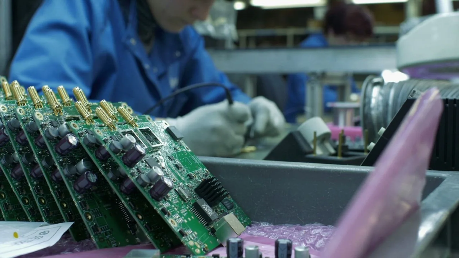
Multi-layer industrial PCBA engineered for electromagnetic compatibility and thermal dissipation

Target Audience

Who Benefits Most from Systems Architecture Design?

Different organizations encounter distinct engineering bottlenecks. We tailor our architectural blueprints directly to your goals.

Hardware Startups & Innovators

The Challenge: Early bench demos running on hobbyist boards (Arduino/Raspberry Pi). Lacking an internal hardware engineering bench, they risk overspending on unviable PCB revisions.

DeviceLab Solution: Feasibility de-risking, comprehensive architectural definition, target BOM modeling, and industrial prototyping ready for venture funding and commercial trials.

Industrial Plants & Manufacturers

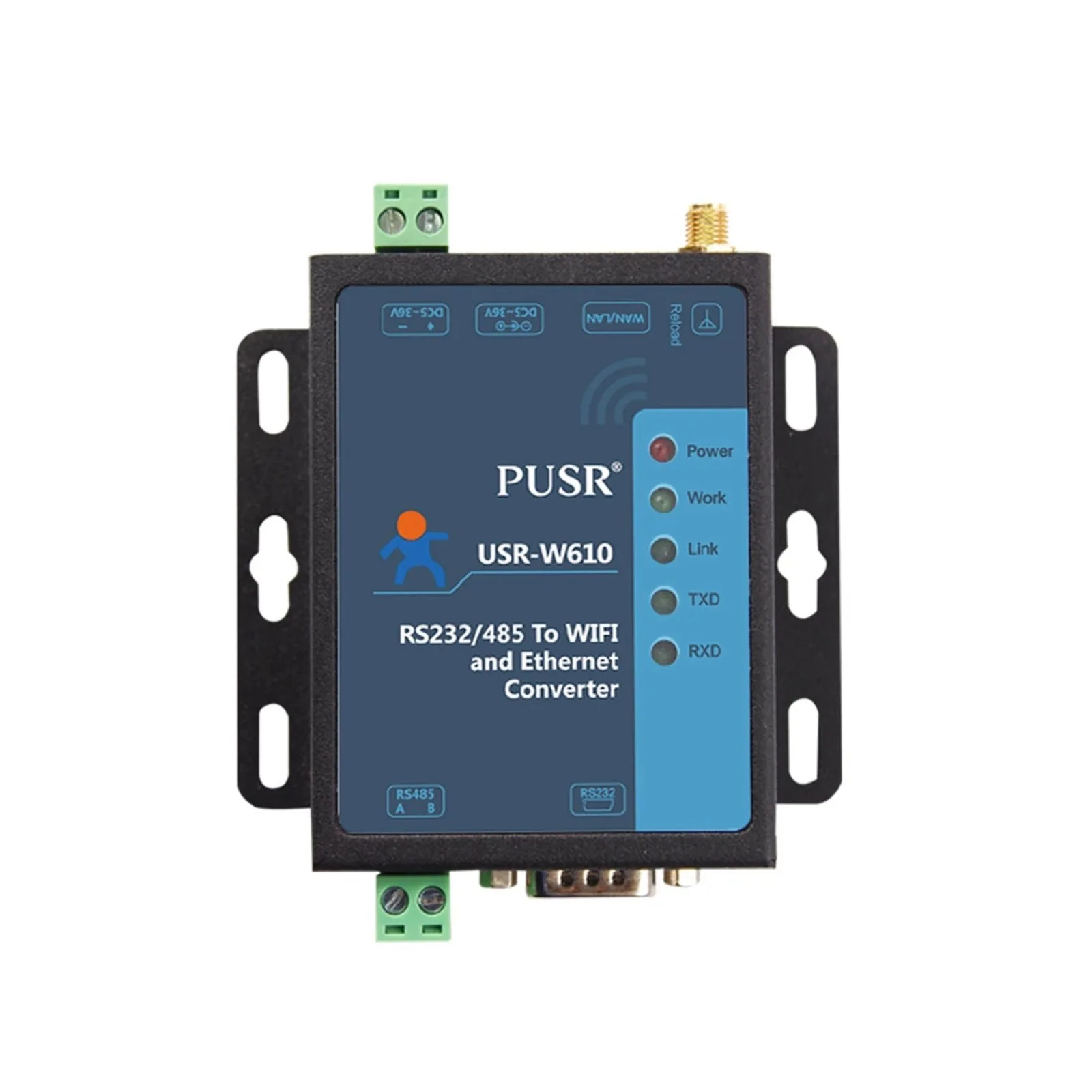
The Challenge: Need to digitize machinery telemetry (legacy Modbus, Siemens/Mitsubishi PLCs). Commercial gadgets don't fit cabinets, speak incompatible protocols, or crash from electrical noise.

DeviceLab Solution: Site surveys, isolated Industrial IoT Gateway architectures, EMI/EMC mitigation, and secure local fieldbus integration into SCADA/MES networks.

System Integrators (SI) & Contractors

The Challenge: Deploying IP audio, automated bells, or access control. Foreign branded equipment is cost-prohibitive, has long lead times, and cannot be customized for local workflows.

DeviceLab Solution: Turnkey OEM/ODM systems architecture (Audio over IP, Smart Campus access), domestic supply chain availability, and full control over device firmware and APIs.

Software Houses & SaaS Teams

The Challenge: Exceptional Web, Mobile, and Cloud engineering, but disconnected from physical electronics: hardware drops offline, firmware locks up, or no secure OTA pipeline exists.

DeviceLab Solution: Closing the physical loop: hardware engineering, deterministic low-level firmware, and standardized MQTT/JSON schemas matching your cloud backend seamlessly.

COTS · OEM · Custom

Not Every System Requires a Ground-Up Circuit Design

We never assume that every project warrants custom silicon layout. The optimal engineering choice satisfies your functional criteria with the lowest cost, schedule, and technical risk.

Criteria 1. Commercial Off-The-Shelf (COTS) 2. Platform Customization (OEM / SOM) 3. Full Custom Development
Nature Leverage certified, commercially available industrial equipment. Utilize proven System-on-Modules (SOM / Compute Modules), customizing carrier boards and firmware. Engineered from schematics, discrete multi-layer PCB layout, and custom enclosures.
When to Choose Standard protocols (Modbus, Ethernet), urgent deployment needed in 1–2 weeks. Proprietary brand identity and tailored I/O needed, but wanting to bypass high-speed CPU routing risks. Strict constraints: ultra-thin mechanical envelope, multi-year battery life, or high volume (>1,000 units).
Advantages Fastest time-to-market, zero hardware NRE, market-proven reliability. Cuts R&D schedule by 50%, eliminates high-speed memory layout risks, simplifies future CPU upgrades. 100% technological sovereignty, zero redundant components, lowest unit production cost (BOM).
Trade-offs & Risks Higher per-unit cost at scale; vulnerable to third-party vendor discontinuations. Partially dependent on SOM supplier roadmap and supply chain allocations. Higher upfront engineering investment (NRE) and longer validation cycle.

We recommend the path that best matches your timeline and business economics—never forcing a one-size-fits-all approach.

Unified Architecture

Designing the Complete System, Not Just an Isolated Board

A hardware device is merely one node in an interconnected chain. We engineer the complete lifecycle of how hardware, firmware, network telemetry, edge AI, and enterprise software interact.

Hardware system instrumentation and test benches at DeviceLab

Layer 1: Device & Sensor Physical Layer

Sensors, signal conditioning, ADCs, camera sensors, and actuators matched to real-world accuracy and measurement dynamics.

Layer 2: Connectivity & Protection

High-voltage TVS surge protection, optical galvanic isolation for RS485/CAN, and industrial Ethernet, Wi-Fi, 4G LTE, BLE.

Layer 3: Edge Processing & Inference

Localized edge computation, signal filtering, TinyML/AI inference, and non-volatile Flash/FRAM caching during network outages.

Layer 4: Platform & Fleet Management

Heartbeat telemetry monitoring across hundreds of distributed nodes, remote diagnostics, and fail-safe dual-bank OTA updates.

Layer 5: Application & Integration

Responsive Web Dashboards, real-time threshold alerts, and open REST/MQTT APIs for enterprise ERP/MES integration.

Decisions made at one layer ripple across the entire system. We design every layer in unison from day one.

Methodology

Structured 4-Phase Systems Engineering Workflow

You don’t need an exhaustive technical spec to start. Our structured process brings clarity, predictability, and velocity to your project.

01

Field Constraints & Briefing

  • Functional Specs
  • Harsh Environments
  • Power Budget
  • User Workflow
02

Architecture & Partitioning

  • HW / SW Boundaries
  • Dataflow Schemas
  • Network Protocols
  • Security Architecture
03

COTS / OEM vs. Custom & BOM

  • Path Evaluation
  • Silicon Qualification
  • Target BOM Costing
  • Time-to-Market Model
04

Detailed Specifications & ICD

  • System Block Diagrams
  • Interface Control Doc
  • Failure Recovery
  • Verification Metrics
Bench prototype electronic board undergoing bring-up and signal integrity measurements

Tangible Deliverables

What You Receive Upon Completion of System Design

1. System Architecture Diagram

Comprehensive schematic of control signals, dataflows, power rails, and protocol interfaces between hardware nodes, gateways, servers, and apps.

2. Detailed Technical Specification (Spec Sheet)

Rigorous documentation defining silicon parameters, electrical power budgets, environmental ratings, and mechanical IP sealing standards.

3. Interface Control Document (ICD)

Explicit serialization standards, payload definitions, register maps, and network protocols (MQTT JSON, Modbus registers, REST APIs) governing all communications.

4. Target BOM Costing Model

Granular Bill of Materials identifying primary silicon, verified suppliers, and unit production cost projections across 100, 1,000, and 10,000 unit tiers.

5. Verification & Risk Mitigation Plan

Systematic matrix of thermal, electrical noise, network dropout, and firmware watchdog validation tests required prior to field deployment.

6. Development Roadmap & Budget

Milestone-by-milestone schedule outlining PoC bench bring-up, PCB layout, prototype SMT assembly, firmware sprints, and pilot field trials.

Proven Case Studies

System Architectures Powering Active Deployments

Discover how DeviceLab engineers complex technical criteria into rugged, field-operating commercial platforms.

View All Case Studies

Edge AI Box — Real-Time Computer Vision & Edge Inference

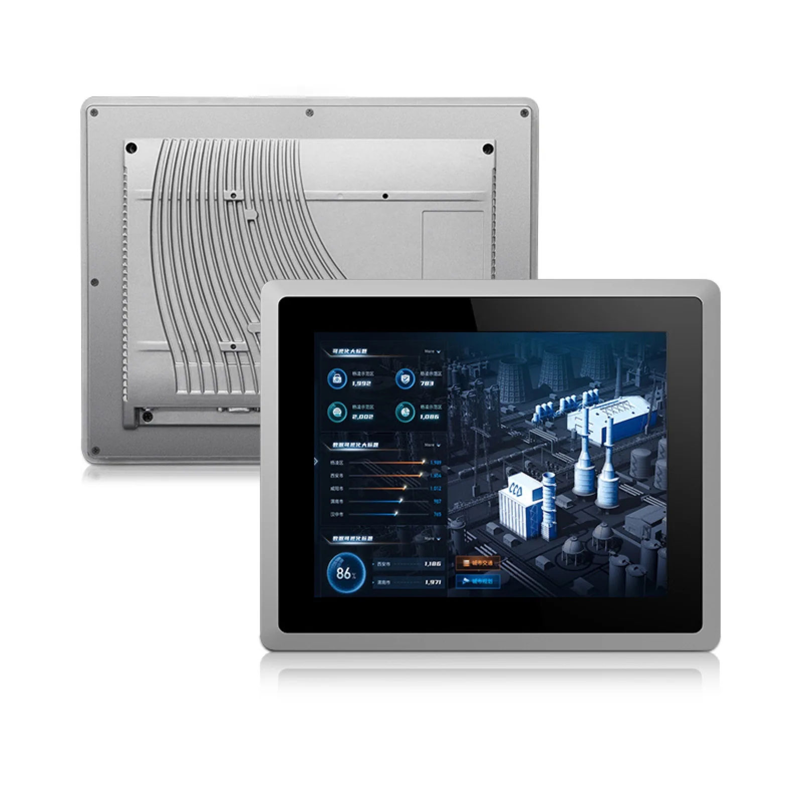
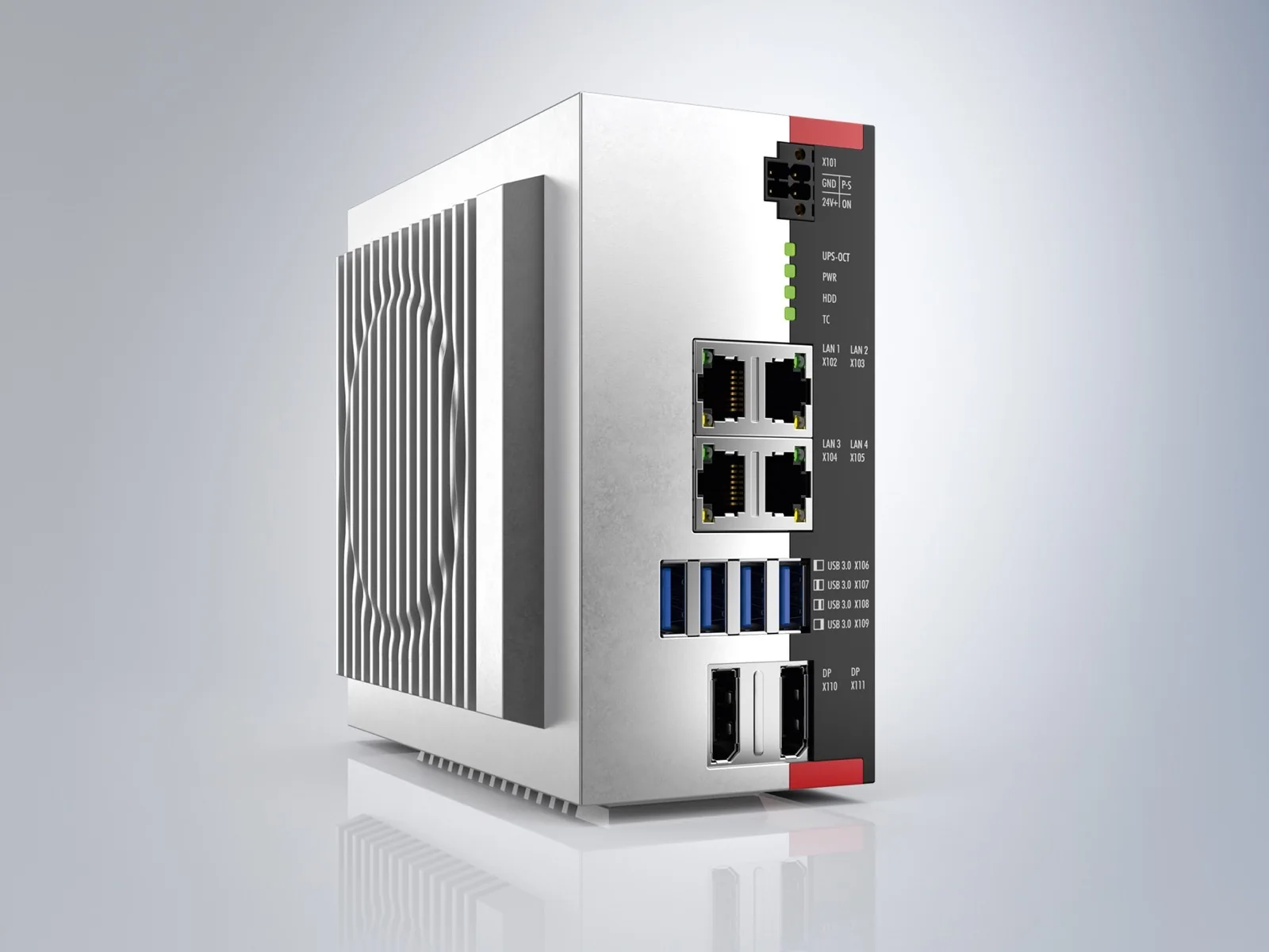
Edge computing hardware architecture featuring onboard NPU. Executes local vision models under 50ms for automated defect inspection (QC) and workshop safety without internet dependency.

  • System Design
  • Edge AI
  • Computer Vision
  • Industrial PC

Systems Engineering Insights

Field-tested methodologies from DeviceLab senior engineers: workload partitioning, fail-safe store-and-forward buffers, industrial bus benchmarking, and thermal design:

View All Technical Articles →

Technical Clarifications

Frequently Asked Questions on System Design

1. We do not have an electrical schematic or formal engineering CAD. Can we engage DeviceLab?

Yes, absolutely. Over 70% of our clients engage DeviceLab at the functional brief or prototype concept stage. The System Design phase is specifically structured to bridge that exact void: we translate your high-level business goals into rigorous technical specifications, hardware block diagrams, timeline estimates, and preliminary BOM budgets.

2. How are system design consulting costs structured?

System architecture engagements are priced on a transparent, milestone-based, fixed-scope proposal determined by technical complexity and peripheral integration requirements. We provide a firm quote upfront with zero hidden fees and deliver self-contained, standalone engineering deliverables.

3. What is the typical timeline for an end-to-end System Design phase?

For standard IoT or embedded telemetry products, the System Design phase spans 2 to 4 weeks. For high-density multi-tiered systems (distributed edge AI, multi-zone IP audio, or complex industrial fieldbuses), it spans 4 to 6 weeks, including preliminary lab bench feasibility evaluations.

4. Is custom PCB layout mandatory, or do you evaluate off-the-shelf options?

We never force a custom PCB. DeviceLab objectively evaluates 3 paths: Commercial Off-The-Shelf (COTS) equipment, customized System-on-Modules (SOM/OEM), and ground-up Custom Development. We only recommend custom hardware when required by mechanical dimensions, battery longevity, or volume unit BOM economics.

5. Who owns the Intellectual Property upon completion of the System Design phase?

You retain 100% full ownership of all architectural block diagrams, Interface Control Documents (ICD), technical specifications, and BOM models developed under the contract. You are free to manufacture internally, pitch investors, or transfer files to any global production facility.

6. Does DeviceLab transition from System Design into prototype fabrication and mass manufacturing?

Yes. System design is the foundational blueprint. DeviceLab delivers turnkey follow-through: Custom Electronic Device R&D, Embedded Firmware, Prototype SMT Assembly, Pilot Production runs (10–100 units), custom mechanical enclosures, and volume manufacturing management.

7. How do you ensure hardware reliability in high-dust, high-temperature, and noisy industrial factory environments?

Reliability is engineered at the architectural level: selecting wide-temperature components (-40°C to +85°C), optical galvanic isolation, high-energy TVS surge clamp diodes, common-mode chokes, and IP65/IP67 enclosures engineered with passive thermal dissipation.

8. Will the device continue to operate if the internet connection or cloud server goes offline?

Yes. All system architectures designed by DeviceLab adhere strictly to a Local-First autonomous operating principle. Control logic, telemetry sampling, and AI inference execute autonomously on the local edge hardware. Data is safely cached in onboard non-volatile memory (Flash/FRAM) and automatically reconciled with the cloud once connectivity is restored.

9. We already have an established backend API or SaaS platform. Can DeviceLab design hardware to interface with it?

Extremely well. We review your API documentation, data schemas, and authentication methods (REST, WebSockets, MQTT broker, TLS/SSL certificates), designing hardware and firmware that serialize data precisely to your platform's specifications.

10. What should we prepare to kick off a System Design engagement with DeviceLab?

You only need a concise briefing addressing 4 questions:
1. What is the core function of the device or system?
2. What is the operating environment and who are the end users?
3. What peripheral machinery, sensors, or software platforms must it integrate with?
4. What are your target production volume and launch timeline?
Our engineering leads review your brief and respond with technical feedback within 24 business hours.

Have an Engineering Challenge Requiring Sound Architecture Before Capital Allocation?

Do not commit capital to premature hardware procurement or drafting without an overarching system architecture. Consult directly with DeviceLab senior engineers to validate feasibility, de-risk failure modes, and determine the optimal technical execution path.