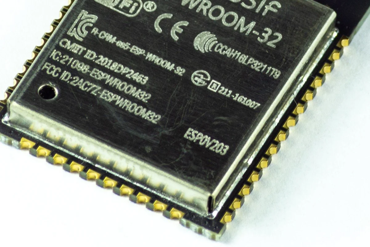
Bill of Materials (BOM) cost optimization is the systematic engineering review and redesign process of analyzing an electronic product's component roster, fabrication specifications, and assembly techniques to reduce unit manufacturing costs (COGS) by 20% to 40% while preserving or enhancing product reliability, performance, and international quality standards.
This technical guide is part of DeviceLab's comprehensive engineering handbook on custom IoT device design and engineering.
In electronic hardware commercialization, the difference between a profitable hardware venture and commercial bankruptcy is often determined by pennies on the BOM. Many engineering teams develop outstanding prototypes that function flawlessly, only to discover that unit manufacturing costs exceed wholesale market pricing. Redesigning after tooling up is agonizing and expensive.
This technical guide analyzes the cost breakdown of commercial hardware, details 5 engineering traps that artificially inflate PCBA costs, presents DeviceLab's 4 golden BOM reduction strategies, and explains how to optimize supply chains across pilot and mass-manufacturing volumes.
What is Electronic Device BOM Cost? Hardware Cost Breakdown
A Bill of Materials (BOM) is the comprehensive list of raw components, silicon ICs, passive parts, mechanical fasteners, PCB laminates, and packaging materials required to assemble a finished commercial product.
In typical commercial IoT and embedded hardware, the Total Cost of Goods Sold (COGS) divides into four distinct cost categories:
                        Finished Product Cost Structure (COGS)
                                        │
     ┌──────────────────────┬───────────┴───────────┬──────────────────────┐
     ▼                      ▼                       ▼                      ▼
[Electronic BOM]     [Bare PCB Board]        [SMT Assembly & Test]  [Mechanical Enclosure]
  (50% - 65%)          (10% - 15%)             (10% - 15%)            (15% - 25%)
 ┌────────────────┐   ┌───────────────────┐   ┌──────────────────┐   ┌───────────────────┐
 │ MCUs, Modems   │   │ Layer count, FR4, │   │ Stencil, machine │   │ Tooling, CNC/Mold,│
 │ Passives, PMIC │   │ surface finish    │   │ setup, placement │   │ screws, packaging │
 └────────────────┘   └───────────────────┘   └──────────────────┘   └───────────────────┘
Optimizing the BOM requires holistically analyzing component selection, board stackups, and assembly logistics rather than simply squeezing distributor component prices.
Cost Optimization Strategies by Production Volume
Cost reduction tactics must align strictly with your current production volume to maximize return on engineering investment:
| Production Volume | Primary Strategic Objective | Hardware Engineering Strategy | Supply Chain & Sourcing Focus |
|---|---|---|---|
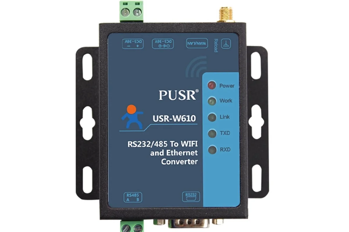
| Prototyping & Pilot Runs (100 – 1,000 units) | Speed to market and firmware validation; minimizing tooling NRE costs | Utilize proven pre-certified wireless modules (ESP32, Quectel); standard 4-layer PCB with standard 6/6 mil trace tolerances | Procure authentic reels via franchised catalog distributors (Digi-Key, Mouser, LCSC); 3D print or CNC machine enclosures |
| Mid-Volume Commercial Production (5,000 – 20,000 units) | Aggressive BOM reduction; maximizing unit gross profit margins | Standardize passive component values; design dual-footprints for critical ICs; migrate 100% of connectors to automated SMD | Negotiate direct pricing with authorized regional component distributors; invest in aluminum injection mold tooling for enclosures |
| High-Volume Mass Manufacturing (>50,000 units) | Fractional-cent optimization; zero-defect high-speed assembly yield | Transition from pre-certified modules to discrete Chip-Down designs; optimize PCB panellization to eliminate laminate scrap | Establish factory-direct supply contracts with semiconductor fabs; automated high-speed in-circuit testing (ICT) jigs |
5 Engineering Traps That Double Hardware Manufacturing Costs
Even veteran engineers often fall into costly design traps during product development:
1. Over-Engineering Specifications
Specifying an industrial quad-core ARM Cortex-A7 processor with 1GB RAM to execute basic temperature logging and relay control. Replacing an over-specified $12 SoC with a purpose-fit $1.20 32-bit Cortex-M0+ or ESP32-C3 immediately eliminates $10 per unit.
2. Component Value Proliferation (Too Many Passive Values)
A circuit board featuring 40 resistors with 25 distinct resistance values ($1 ext{k}Omega$, $1.2 ext{k}Omega$, $2.2 ext{k}Omega$, $4.7 ext{k}Omega$, $5.1 ext{k}Omega$, $10 ext{k}Omega$). Each unique component value requires its own feeder slot on the SMT pick-and-place machine, inflating feeder setup fees and inventory complexity. Consolidating passive components down to 5–8 standardized E-series values slashes setup overhead.
3. Sole-Source Proprietary Silicon
Designing around a proprietary sensor or power management IC manufactured by a single boutique vendor with no drop-in alternatives. When shortages hit, spot-market brokers price-gouge the part from $1.50 to $45, completely halting production.
4. Excessively Tight Mechanical and PCB Tolerances
Specifying unnecessary 3/3 mil trace/space or blind/buried microvias on a simple microcontroller board forces PCB fabricators to use expensive laser-drilling and high-density interconnect (HDI) processes, tripling bare board costs. Designing to standard 5/5 mil rules ensures low-cost fabrication across all standard board houses.
5. Excessive Manual Connectors and Hand-Soldered Cables
Using multiple expensive pin headers, terminal blocks, and custom wiring harnesses that require manual post-assembly hand soldering. Replacing multi-board assemblies with a single unified PCB slashes labor and eliminates human wiring errors.
4 Golden Strategies to Slash BOM Costs by 30% at DeviceLab
DeviceLab applies disciplined Value Engineering to drive down hardware production costs:
Strategy 1: Dual-Footprint & Second-Source Layout Architecture
During PCB layout, our engineers design overlapping dual-footprints for critical components (such as SOIC-8 alongside WSON-8 footprints, or STM32 footprint compatible with alternative pin-to-pin MCUs from GigaDevice or Geehy). During production, purchasing teams flexibly procure whichever silicon is available at the lowest market spot price without modifying the board layout.
Strategy 2: 100% Transition from Through-Hole (THT) to Surface Mount (SMD)
Every hand-soldered through-hole component requires human labor after the board exits the reflow oven. Hand-soldering 10 through-hole pins often costs more than automated SMT placement of 100 SMD components. Transitioning 100% of connectors, LEDs, switches, and passives to SMD enables fully automated, touch-free production.
Strategy 3: PCB Dimension & Panellization Optimization
We review PCB physical layouts to shrink surface area by 20% to 30%. On standard manufacturing panels (600x500mm), shrinking board dimensions allows fabricators to increase yields from 40 boards to 60 boards per panel, directly cutting raw PCB costs by 33%.
Strategy 4: Direct Franchised Supply Chain Sourcing
DeviceLab connects clients directly to authorized component distributors. Purchasing components in full manufacturer reels (3,000 to 5,000 units per reel) secures volume price discounts of 40% to 60% compared to cut-tape prototype purchases.
DeviceLab BOM Teardown & Cost Reduction Consulting Services
If your hardware product design is finalized but production costs are too high to achieve target profit margins: * BOM Teardown & Cost Driver Analysis: Line-by-line engineering audits identifying primary cost drivers, obsolete components, and excessive supplier markups. * Cross-Reference Component Selection: Delivering verified cross-reference lists of drop-in alternative components from top-tier Asian and international semiconductor manufacturers, cutting unit prices by 30% to 50%. * PCB Redesign for Cost (DFM/DFA): Redesigning schematics, optimizing routing layers, condensing board surface area, and assembling pilot verification batches to confirm zero performance loss.
Frequently Asked Questions (FAQ)
1. Does using lower-cost alternative components compromise device reliability?
Not when specifying qualified industrial-grade alternatives. BOM optimization is not about buying counterfeit parts from flea markets. It is the disciplined replacement of overpriced Western brands with verified components from accredited semiconductor fabricators (including top-tier Taiwanese, Korean, and Japanese manufacturers certified to automotive AEC-Q standards). All candidate alternatives undergo rigorous laboratory bench testing prior to production release.
2. When is the ideal milestone to execute BOM cost optimization?
The optimal window is immediately after the first Engineering Validation Test (EVT) prototype is functional, and prior to committing capital to mass-production tooling (DVT / Pilot run). Optimizing at this juncture prevents expensive enclosure re-tooling and avoids market launch delays.
3. How long does a typical BOM optimization review take?
A comprehensive BOM teardown and component cross-referencing audit requires 3 to 7 business days. If the project necessitates PCB re-layout, prototype fabrication, and functional re-validation, the full engineering cycle requires 2 to 3 weeks.
4. How does plastic injection molding tooling affect per-unit enclosure costs?
Industrial injection molds require substantial upfront NRE tooling capital ($2,000 to $10,000+ depending on cavity count and mechanical complexity): * At 100 units: Tooling amortization adds $20–$50 per unit (cost-prohibitive; 3D printing or CNC machining is preferred). * At 10,000+ units: Tooling amortization drops to pennies per unit, while the raw plastic shot cost is only $0.50–$1.50 per enclosure—over 10x cheaper than 3D printing.
5. Why is "Second-Sourcing" a critical engineering requirement?
Second-sourcing means engineering a circuit position so that at least two pin-compatible components from different semiconductor manufacturers can drop into the PCB without schematic or software changes. During global chip shortages, companies with second-source designs maintain continuous factory production while single-source competitors shut down.
6. Why are 0402 SMD passive components cheaper than 0805 packages?
The 0402 package (1.0mm x 0.5mm) consumes significantly less ceramic and precious metals than 0805 (2.0mm x 1.25mm). Furthermore, a standard 7-inch reel holds 10,000 pieces of 0402 (compared to only 4,000 pieces of 0805), dramatically reducing manufacturer packaging, storage, and air freight expenses.
7. Does DeviceLab commit to specific cost reduction percentages?
Yes. Upon receiving your existing schematic package and BOM list, our engineering team executes a preliminary audit and provides a guaranteed target cost reduction range (typically 15% to 35%) prior to executing formal service agreements.
Lower Hardware Production Costs & Accelerate Market Profitability
Is your hardware product engineered to compete profitably in the global marketplace?
👉 Submit Your BOM & Schematics for an Optimization Audit
Consult directly with DeviceLab's Hardware Supply Chain Engineering Team via Hotline/WhatsApp/Zalo: 0982.503.355.