Securing a reputable, professional electronic circuit design and hardware R&D company in Hanoi is a make-or-break strategic decision for technology enterprises, hardware startups, and industrial machinery manufacturers. A production-ready printed circuit board design must transcend tabletop Proof-of-Concept (PoC) breadboards; it must satisfy stringent electromagnetic compatibility (EMC/ESD) standards, optimize for high-volume Design for Manufacturing (DFM), incorporate globally available long-lifecycle components, and guarantee 100% intellectual property (IP) protection for the client.
This technical guide is part of DeviceLab's comprehensive engineering handbook on custom IoT device design and engineering.
📌 5 Essential Criteria for Selecting a Hardware R&D Partner (Key Takeaways):
- Full Native Source File Delivery: Avoid vendors who retain source CAD files to trap clients into captive, inflated manufacturing contracts.
- Proven Industrial Noise Immunity (EMC/ESD) Competency: Solid continuous ground planes, multi-stage LC power filtering, transient TVS suppression diodes, and galvanic optical isolation on fieldbus interfaces.
- Lifecycle-Aware BOM Component Management: Specifying MCUs and power management ICs from tier-1 global manufacturers (STMicroelectronics, Texas Instruments, Microchip, NXP) with verified 10+ year lifecycles in stock at franchised distributors (DigiKey, Mouser, LCSC).
- In-House Rapid Prototyping Facilities: Dedicated SMT assembly lines and hardware test laboratories in Hanoi that compress the timeline from initial schematic freeze to running hardware down to 10 - 14 days.
- Pre-Compliance Regulatory Support: Guidance and execution of pre-compliance EMI/EMC testing for Vietnamese QCVN certification as well as international CE/FCC export compliance.

4 Critical Pitfalls When Engaging Inexperienced Circuit Designers
1.1. Boards That Pass Benchtop Tests but Freeze in the Factory (EMI Noise)
An amateur hobbyist or fresh graduate can easily build an ESP32 or Arduino board that blinks LEDs on an office desk. However, once installed in a factory switchboard adjacent to variable frequency drives, heavy magnetic contactors, and high-power hydraulic pumps, electrical fast transients (EFT) couple into trace loops, locking up the CPU or causing perpetual brownout resets. A professional R&D partner in Hanoi like DeviceLab adheres to disciplined 4-layer stackups (Signal - GND - Power - Signal), continuous copper pour shielding, and dedicated ferrite choke stages.
1.2. Specifying Obsolete Components or Gray-Market Parts
Inexperienced designers frequently select cheap components from local retail shops without verifying their product lifecycle (End-of-Life - EOL) on global supply databases. When a company prepares to ramp to commercial production of 1,000 units, they are suddenly blindsided by 52-week lead times or obsolescence notices on primary silicon, forcing costly ground-up redesigns.
1.3. Vendor Lock-In via Withheld CAD Files
A prevalent vendor trap involves quoting deceptively low design fees, only to deliver compiled binary firmware (.hex/.bin) and bare Gerbers upon completion. When the client later needs to reassign a single sensor pin or add an auxiliary interface, the vendor demands exorbitant change fees.
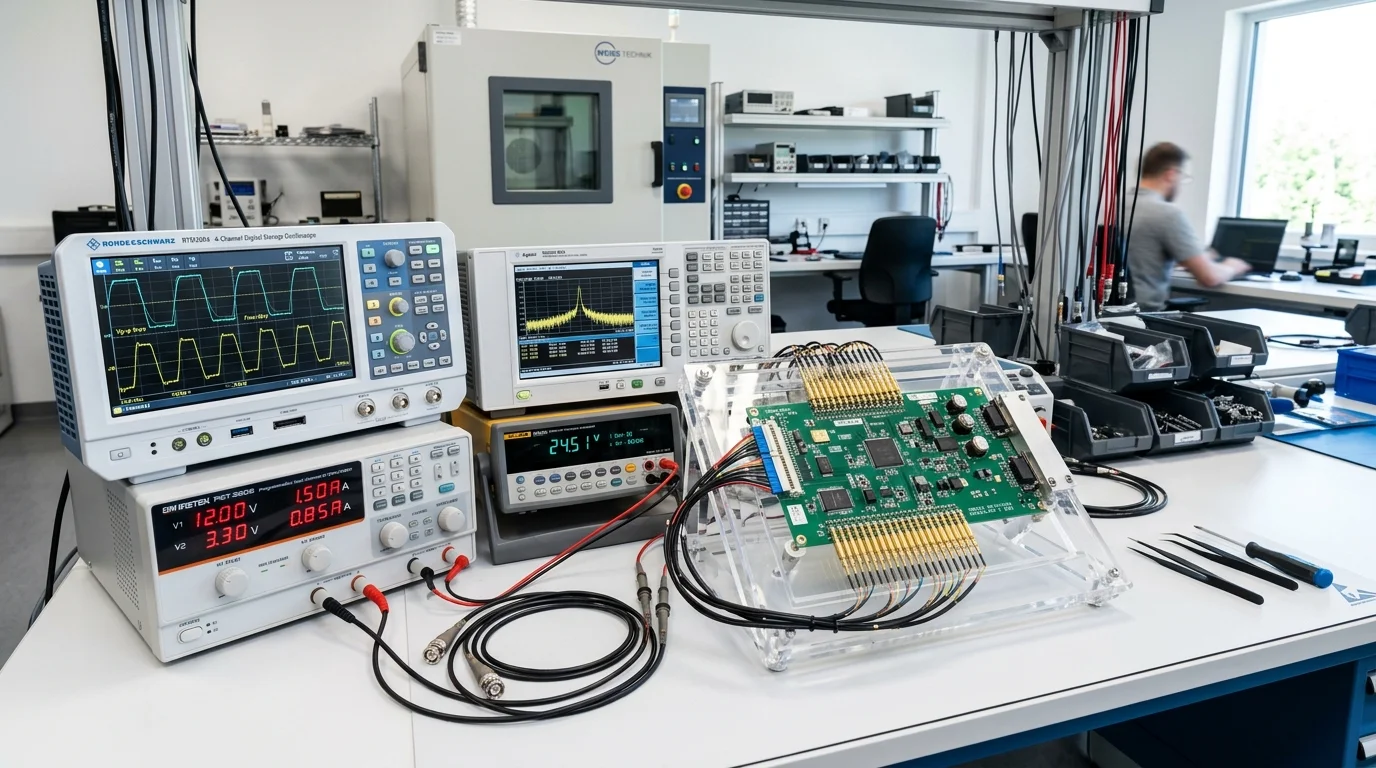
6-Stage Standard Hardware Engineering Process at DeviceLab Hanoi
To ensure prototype first-pass yield exceeds 95% on initial board revisions (Rev 1.0), DeviceLab executes a structured 6-stage engineering lifecycle:
| HARDWARE R&D LIFECYCLE AT DEVICELAB HANOI |
+-----------------------------------------------------------------------------------+
| STAGE 1: Technical Scoping, NDA Execution & Product Requirements Document (PRD) |
| |
| STAGE 2: Schematic Capture & Global Sourcing BOM Optimization |
| |
| STAGE 3: Multi-Layer PCB Layout (Controlled Impedance, DFM & EMI Rules) |
| |
| STAGE 4: Bare PCB Fabrication & Automated Surface Mount (SMT) Assembly in Hanoi |
| |
| STAGE 5: Board Support Package (BSP) Bring-up, Functional Validation & Burn-in |
| |
| STAGE 6: Operational Prototype Delivery & Complete 100% IP CAD Source Handover |
+-----------------------------------------------------------------------------------+

Transform Your Device Concept into Reality with DeviceLab
We accompany enterprise partners from initial concept, schematic design, and firmware engineering through to mass turnkey PCBA manufacturing. Clear contracts, guaranteed timelines, and complete intellectual property ownership.
Chief Engineering Officer: (+84) 982.503.355