
R&D Strategy
IoT Hardware R&D Cost Analysis: In-House vs Outsourcing ODM
Comprehensive economic breakdown comparing engineering team overhead, CAD tool licenses, laboratory test equipment versus turnkey ODM partnership.
Engineering Lifecycle
Transparent, step-by-step custom electronic device and system engineering.
We guide you across requirements capture, architecture design, functional prototyping, pre-compliance testing, and volume manufacturing.
Overall Methodology
Requirement
Clarify functional specifications, operating environment, target BOM cost, and regulatory standards.
System Design
Establish hardware block diagrams, select MCU/MPU platforms, communication protocols, and cloud interfaces.
Engineering
Schematic capture, multi-layer PCB layout, low-level firmware coding, and 3D mechanical enclosure modeling.
Prototype
Rapid SMT board assembly, lab bring-up, firmware testing, and real-world operational validation.
Testing
Thermal testing, power surge/EMI screening, BOM supply chain de-risking, and manufacturing yield optimization.
Pilot
Assembling pilot batches (10 to 100 units), custom functional test jig (FCT) calibration, and QC checklists.
Production
Mass production transition, pre-compliance certification, packaging, and remote OTA firmware lifecycle support.
Getting Started
Simply describe what your device or connected system needs to achieve. Our senior engineers analyze technical feasibility, recommend platforms, and define the development milestones.
Flexible Delivery Paths
 01
01
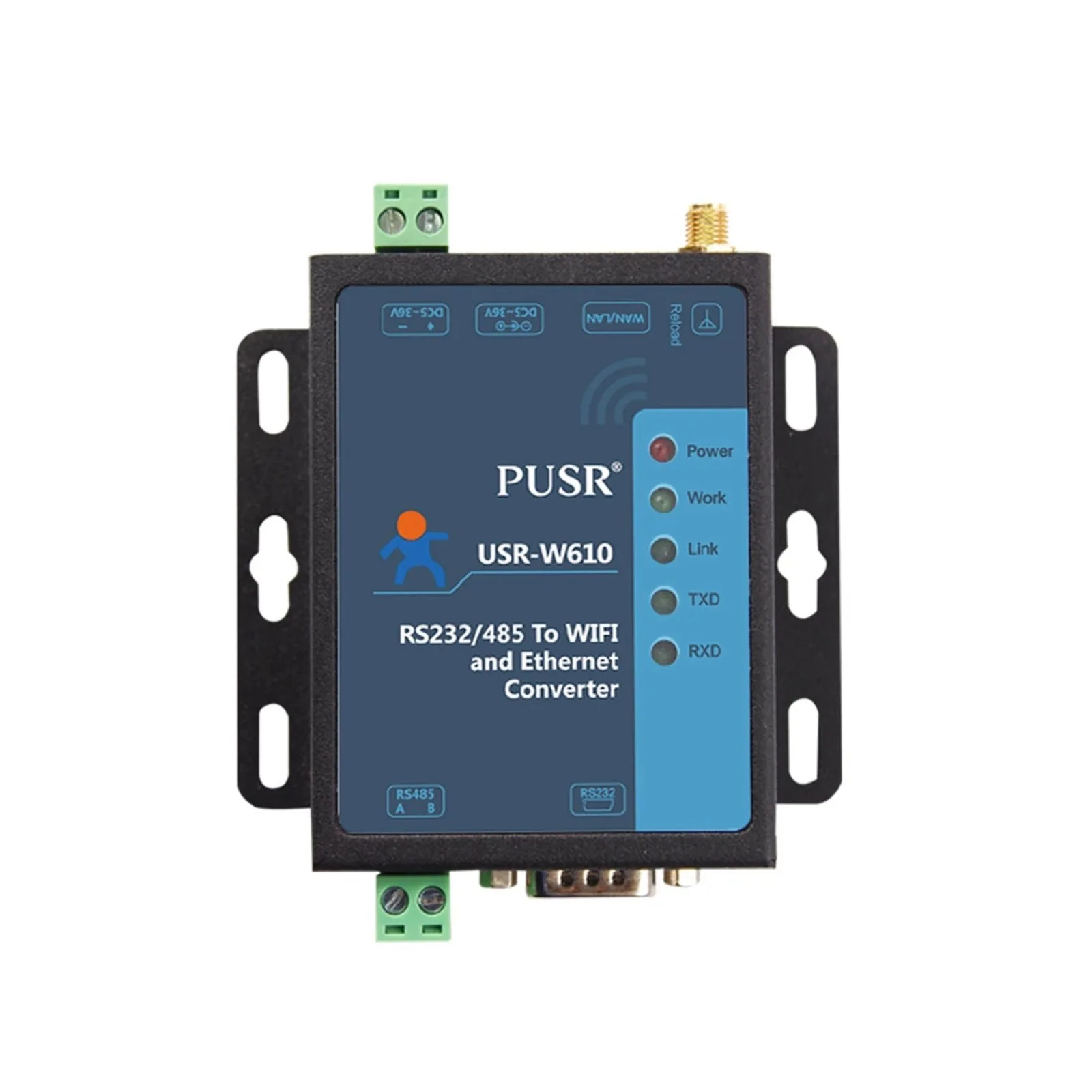
When reference devices exist → Customization, firmware adaptation & system integration
 02
02
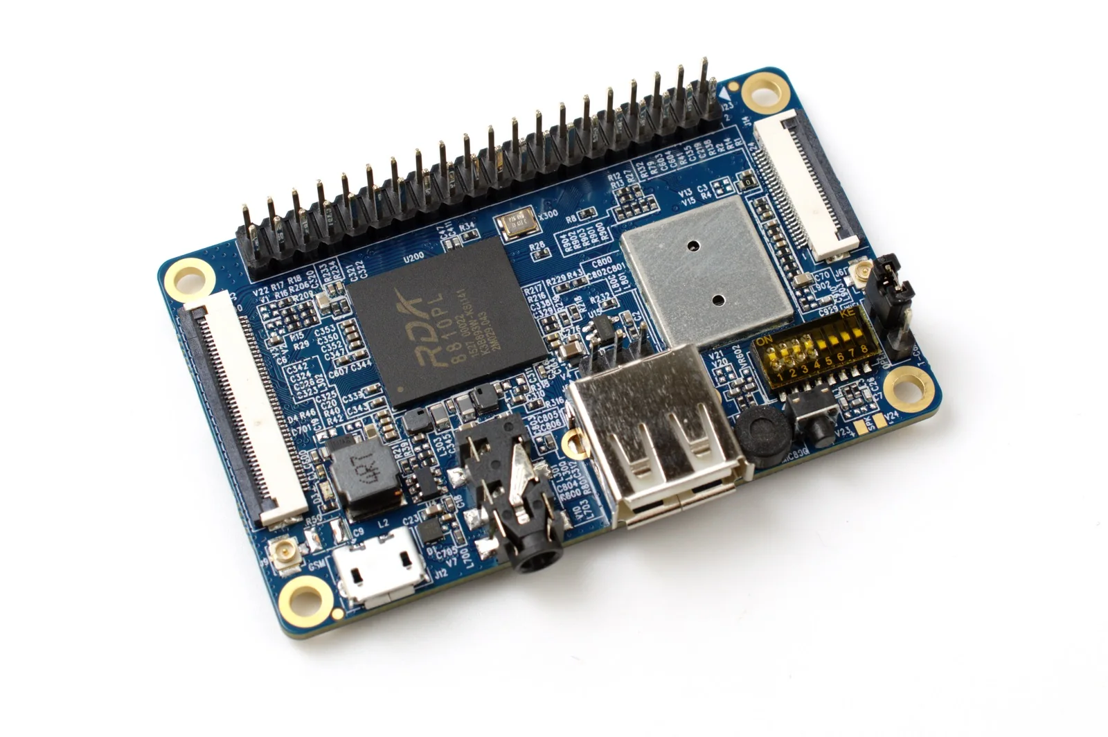
When standard computing modules fit → Custom carrier board and dedicated enclosure engineering
 03
03
When proprietary specifications require a ground-up design → Custom schematics, PCB, and firmware
Our goal is choosing the optimal path tailored to your budget, time-to-market, and production scale.
Project Governance
Critical milestones are bench-tested and formally approved before transitioning to the next phase.
End Deliverable
Our mission is transforming your technical concept into a field-proven, fully documented, and volume-manufacturable product.
ENGINEERING INSIGHTS & BEST PRACTICES
Detailed engineering analyses on hardware R&D economics, laboratory-to-field reliability testing, fail-safe firmware architecture, and IP transfer standards.
Comprehensive economic breakdown comparing engineering team overhead, CAD tool licenses, laboratory test equipment versus turnkey ODM partnership.
Comprehensive breakdown: 2.5kV galvanic surge simulation, 72-hour thermal burn-in at 65°C, continuous vibration, and ESD immunity.
Designing zero-brick remote firmware updates over cellular/Ethernet with cryptographic validation and autonomous flash rollback.
Complete checklist of deliverables required for true 100% intellectual property ownership without proprietary vendor lock-in or recurring fees.
PROCESS CLARIFICATIONS
Practical engineering answers covering feasibility assessment, milestone verification, pilot runs, and volume manufacturing.
Before formal commitment, DeviceLab engineers evaluate core IC component lifecycle status, supply lead times, target unit BOM costs, power budgets, and harsh operational constraints. For high-risk aspects, we execute bench feasibility mocks to ensure high-confidence timelines and fixed-scope proposals.
We enforce pin-to-pin drop-in alternatives and dual-footprint PCB routing strategies at the schematic phase. We exclusively prioritize industrial components with guaranteed 10+ year longevity commitments from tier-1 manufacturers, eliminating supply disruption vulnerabilities.
Every engineering milestone is governed by explicit, pre-agreed technical Acceptance Criteria. Sign-offs require concrete verification artifacts: schematic review reports, bench-tested working prototypes accompanied by oscilloscope measurements, and field log data before progressing.
Standard MCU-based industrial IoT devices typically take 4 to 8 weeks to deliver fully assembled SMT prototypes running low-level drivers. Complex platforms (multi-camera Edge AI vision or specialized RF arrays) require 8 to 16 weeks, including rigorous stress testing.
Transitioning directly from a lab prototype to high-volume assembly carries severe yield and tolerance risks. A pilot batch of 10 to 100 units exposes DFM/DFA defects, verifies automatic functional test (FCT) fixtures, and proves assembly yields before capital is committed to volume manufacturing.
① 2.5kV galvanic surge pulses applied to RS485/CAN/Ethernet ports; ② 72-hour continuous thermal chamber burn-in at +65°C under maximum processing load; ③ Sudden power interruption and brown-out flash buffer integrity stress testing; ④ Mechanical vibration endurance testing on solder joints.
Clients receive 100% production-ready engineering packages: native Altium schematics, multilayer PCB Gerber and drill files, structured manufacturing BOMs with exact MPNs, Pick-and-Place coordinates, uncompiled C/C++ firmware source code, 3D mechanical STEP assemblies, and factory FCT testing protocols.
Yes. We integrate rigorous EMC/EMI design best practices (ground plane partitioning, high-frequency filtering, TVS suppression) during PCB layout. We execute pre-compliance near-field spectral scans prior to accredited test lab submission, assisting in technical dossier preparation and debug tuning.
All turnkey hardware manufactured by DeviceLab includes a 24-month standard warranty. Firmware bugs attributable to the agreed design scope are patched free of charge, with options for remote OTA fleet maintenance and enterprise SLA agreements.
Yes, absolutely. Because all intellectual property, BOMs, Gerbers, and firmware source files are 100% transferred to you, you have complete sovereignty to manufacture with any EMS facility globally. We also provide turnkey factory transfer assistance and test jig deployment.
No need for a finished specification document. Tell us about the electronic device or system you want to build.
From operational problem → technical architecture → living physical product.