
Designing an Electronic Functional Circuit Test Fixture (FCT / Bed-of-Nails Pogo-Pin Test Jig) is a mandatory mechatronic quality assurance (QA/QC) engineering milestone when scaling an electronic hardware product from hand-built engineering prototypes (EVT) to volume PCBA mass production (PVT / MP). By aligning an array of spring-loaded Pogo Pins against bottom-side PCB test pads and coupling them with an automated measurement, load-simulation, and switching motherboard, an FCT Test Jig executes pre-power short-circuit screening, automated high-speed firmware flashing, analog/digital/RS485/RF functional loopback verification, and QR serial barcode label printing in just 10 to 25 seconds per board—eliminating 100% of human testing oversight and slashing factory QC labor costs by 80%.
Core R&D & Mass-Production QC Engineering Service for Hardware Startups & OEMs: This technical guide belongs to our Turnkey PCB Fabrication & SMT/THT Assembly (PCBA) and Industrial Electronic Circuit Design (DFM / DFT) cluster. Explore our complete hardware lifecycle workflow in Electronic Device Development from EVT & DVT to PVT Mass Production.
⚡ Technical Quick Fact Sheet: Automated FCT Pogo-Pin Test Fixture Engineering
- Precision Mechanical Architecture: Heavy-duty quick-action
Toggle Clamp (90kg–250kg holding force)with linear ball-bushing guide shafts, CNC-machinedESD Antistatic Bakelite / POM / FR-4 Carrier Plates (±0.02mm tolerance), stainless-steelTapered Tooling Alignment Pins, and a spring-supportedFloating Probe Protection Plate. - Two-Piece Spring-Loaded Pogo-Pin System: Press-fit outer
Receptacles (R75 / R100 / R125)permanently wired inside the fixture base, paired with gold/rhodium-plated inner springPlungers (P75 / P100 / P125)that slide out for 10-second tool-free replacement after100,000 compression cycles. - 5-Stage Automated Test Sequence: (1)
Capacitor Discharge & Pre-Power Short-Circuit Check(measuring 24V/5V/3.3V rail impedance to GND) → (2)OCP Power-Up & LDO/Buck Rail Voltage Verification→ (3)High-Speed Firmware Flashing & Readout Protection Lock (SWD/JTAG/UART)→ (4)Peripheral Loopback Test (DI/DO, 4–20mA, PT100, RS485, 4G/Wi-Fi RSSI)→ (5)Pass/Fail Binning & Zebra QR Label Printing. - Production Throughput & Multi-Up Scaling: Compresses per-board testing time from
12–15 minutes (manual)down to10–25 seconds; supports Multi-Up Panel Jigs testing2x or 4x PCBs simultaneouslyin a single clamp stroke.
📌 Why Design for Testability (DFT) & FCT Jigs Determine the Survival of Mass-Produced Hardware:
- The "Rule of 10" Escalation of Defect Costs in Electronics Manufacturing: Catching a cold solder joint or tombstoned SMD resistor on the FCT Test Jig right after the reflow oven costs
$0.20 USD (5,000 VND)in touch-up rework; catching it after ultrasonic enclosure assembly costs$2.00 USD (50,000 VND); and letting a defective board escape to an industrial customer site costs$200+ USD (5,000,000+ VND)in field warranty travel and brand damage. - Empower General Assembly Operators to Execute Complex Engineering Tests: Highly paid R&D engineers no longer need to sit with oscilloscopes, multimeters, and command-line IDE tools flashing boards one by one. A line operator simply drops the PCB into the nest, pulls the handle, and watches for the green
PASSindicator and automatic barcode label. - Instant Electronic Fuse Protection Saves Assembled Boards from Reflow Shorts: If a newly soldered PCBA has a microscopic solder bridge shorting the 3.3V rail to GND, plugging it into a standard bench power supply will instantly vaporizePCB traces or burn out the MCU. DeviceLab's FCT Jig measures cold rail resistance first and trips its
100μselectronic current limiter before any thermal damage can occur.
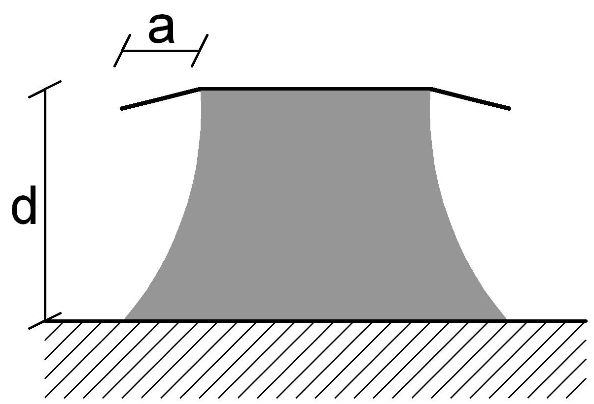
The Production Nightmare of Manufacturing 1,000 PCBA Units Without an Automated Test Fixture
Many IoT hardware startups and industrial equipment OEMs invest months of intense R&D perfecting the schematic, layout, and firmware for their first 5 hand-soldered engineering prototypes. Once those 5 prototypes perform flawlessly on the lab bench, management immediately places a purchase order to SMT-assemble 500 to 2,000 PCBA units for their commercial launch—while completely forgetting to ask: "How are we going to flash firmware, calibrate analog channels, and verify 100% of the I/O ports across 2,000 boards before shipping them to customers?"
Attempting to test a 1,000-unit production batch manually—plugging in a DC power jack, holding a 4-pin SWD programming header against unpopulated pads, clicking "Program" on a laptop, and then using a screwdriver to land individual RS485, 4–20mA current simulator, and 24VDC digital input wires into screw terminals—triggers an immediate manufacturing crisis:
- Crippling Delivery Bottlenecks: Manually wiring, flashing, and testing a multi-channel industrial controller board takes a skilled technician 12 to 15 minutes per unit (capping daily output at roughly 30 to 35 boards per person). Testing a 1,000-board batch consumes 30 full engineer man-days of repetitive wire plugging!
- Mechanical Connector Wear & Lifted Copper Pads on Brand-New Boards: Repeatedly jamming programming headers into board connectors hundreds of times bends contact pins, while tightening and loosening terminal block screws during factory testing strips screw heads on brand-new commercial products before they ever reach the customer.
- High Rate of Escaped Defects Due to Operator Fatigue: After repeating the same monotonous manual test routine 50 times in a single afternoon, even a conscientious technician will inevitably skip testing Channel 7 of an analog input or forget to enable MCU Readout Protection (RDP)—allowing defective or unencrypted boards to receive a "QC Passed" sticker and ship out the door.
Mechatronic, Electrical & Software Architecture of an Industrial FCT Automated Test Station
A production-grade FCT Test Fixture engineered by DeviceLab is far more than a simple acrylic box with spring pins—it is a closed-loop Automated Test Equipment (ATE) workstation integrating three synchronized engineering layers:
| ARCHITECTURE OF DEVICELAB AUTOMATED FCT POGO-PIN TEST STATION (ATE SYSTEM) |
+--------------------------------------------------------------------------------------------------+
|
| [TIER 1: PRECISION CNC MECHANICAL FIXTURE & POGO-PIN BED-OF-NAILS]
| +--------------------------------------------------------------------------------------------+
| | • Toggle Clamp + Linear Ball-Bushing Guide Columns + CNC ESD Bakelite Nest (±0.02mm) |
| | • Asymmetric Poka-Yoke Tooling Pins (Ø3.0mm) + Clamp-Closed Micro-Switch Interlock |
| | • Two-Stage Pogo-Pin Array (Receptacle R100 + Plunger P100) contacting DUT Bottom Testpads |
| +---------------------------------------------+----------------------------------------------+
| | (Probing Power Rails, SWD/UART, Analog & I/O)
| v
| [TIER 2: INTERNAL FCT MEASUREMENT, PROGRAMMING & LOAD-SIMULATION MOTHERBOARD]
| +--------------------------------------------------------------------------------------------+
| | 1. Pre-Power Safety Block: Cold Rail-to-GND Impedance Check + OCP Current-Limited Supply |
| | 2. Multi-Rail Voltage & Current Scanner: Analog Multiplexer + 24-bit ADC (24V/5V/3.3V/Vref)|
| | 3. High-Speed Isolated Flasher: Gang/Single Programmer (SWD / JTAG / UART / ESP / USB DFU) |
| | 4. Peripheral Loopback Simulator: Precision 4-20mA DAC Source, 24V DI Stimulus, RS485 Ping |
| +---------------------------------------------+----------------------------------------------+
| | (USB / Industrial Ethernet / RS232)
| v
| [TIER 3: HOST TEST RUNNER GUI, ZEBRA QR BARCODE PRINTER & CLOUD QC TRACEABILITY]
| +--------------------------------------------------------------------------------------------+
| | • Step-by-Step LSL/USL Pass/Fail Operator Screen + Audible Buzzer + Auto QR Label Trigger |
| | • Full Per-Board Serial/UID Test Log Archiving (CSV / SQLite / Cloud MES Traceability API) |
| +--------------------------------------------------------------------------------------------+
+--------------------------------------------------------------------------------------------------+
Design for Testability (DFT) PCB Layout Rules & Pogo-Pin Selection Matrix
To ensure that an FCT Test Fixture operates with 99.9% first-pass contact reliability across 100,000+ clamping cycles without bent probes or false contact failures, hardware engineers should incorporate DeviceLab's Design for Testability (DFT) Rules directly during the PCB layout stage:
| DFT PCB Parameter & Probe Spec | Recommended Engineering Best Practice | Minimum Acceptable Manufacturing Limit | Practical Mechanical & Production Rationale |
|---|---|---|---|
Exposed Copper Test Pad Diameter (Test Pad Ø) |
Ø 1.2 mm – 1.5 mm (ENIG gold or flat HASL finish, 100% free of solder mask) |
Ø 0.9 mm |
Accounts for cumulative tolerances of CNC drilling in ESD Bakelite (±0.03mm), plunger lateral play under compression, and PCB fabrication registration; ≥1.2mm guarantees dead-center probe landing. |
Center-to-Center Test Point Spacing (Pad Pitch) |
≥ 2.54 mm (100 mil) → Uses rugged P100 (Ø1.36mm) probes |
1.27 mm (50 mil) → Requires delicate P50 (Ø0.68mm) probes |
Standard P100 and P75 (1.91mm pitch) probes have thick, durable barrels rated for 3A–5A continuous current and low unit cost; ultra-thin P50 needles bend easily if an operator misaligns a board. |
Mechanical Alignment Holes (Non-Plated Tooling Holes) |
3x Unplated Holes Ø 3.0 mm (+0.05/-0mm) placed asymmetrically at 3 corners |
2x Holes Ø 2.5 mm at opposite diagonal corners |
Never align a PCB using its routed outer edges because V-cut depaneling and CNC tab-routing vary by ±0.25mm. Three asymmetric tooling holes provide sub-50μm precision and prevent 180° reverse insertion (Poka-Yoke). |
| Clearance from Test Point to Tall Bottom-Side Components | ≥ 3.0 mm |
1.5 mm |
Leaves sufficient structural wall thickness around the probe hole when CNC-milling recessed relief pockets in the bottom carrier plate for bottom-side SMD components. |
Pogo-Pin Plunger Tip Geometry (Tip Style) |
4-Point Crown Tip (Style B) for flat SMD test pads; 9-Point Serrated Tip (Style Q) for THT leads |
Single-Point Spear Tip (Style A) reserved only for open vias |
4-point crown tips self-clean and pierce thin rosin flux films without trapping insulating flux residue in a central valley or sliding off solder domes. |
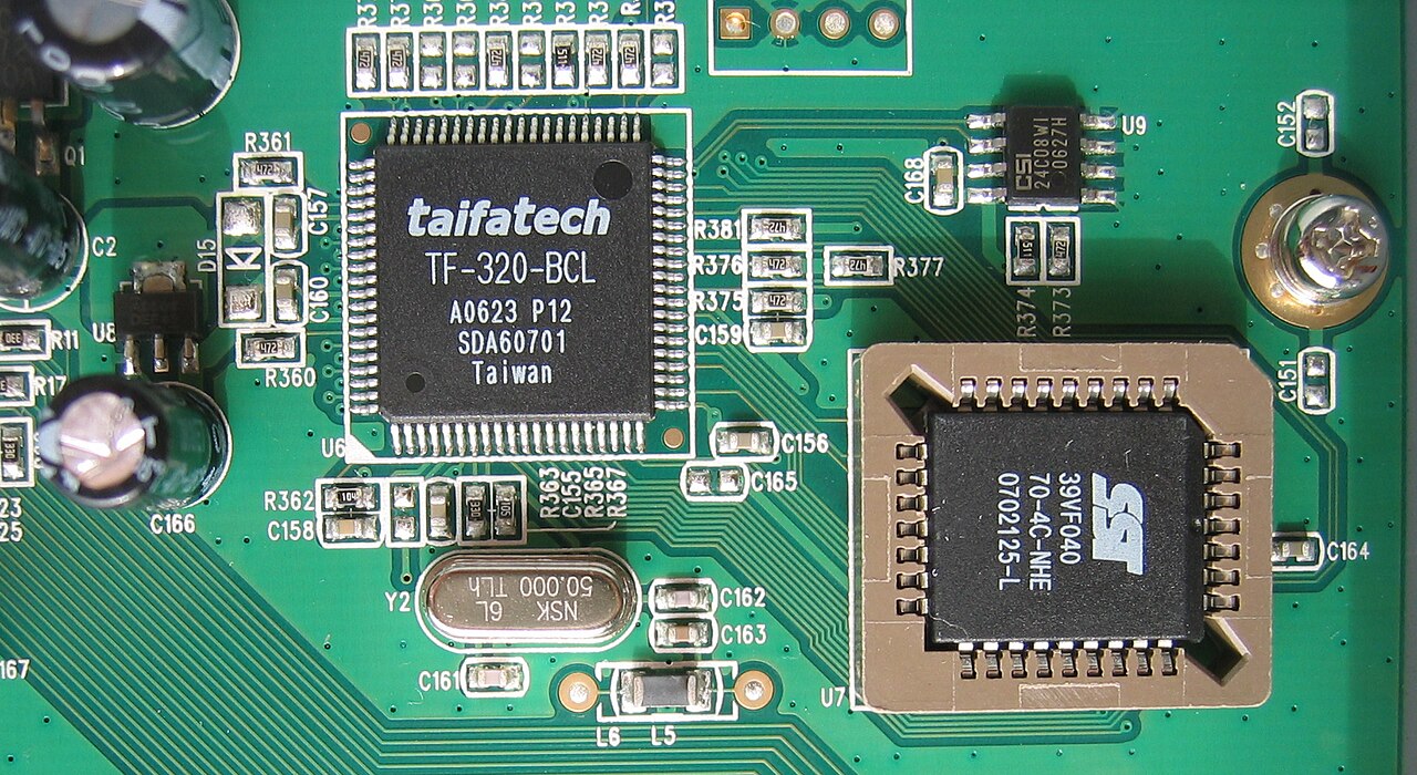
Automated FCT Test Script Structure & Quantitative LSL/USL Factory QC Logging
Inside every FCT Test Station delivered by DeviceLab, the automated test sequence is governed by a deterministic specification table defining explicit Lower Specification Limits (LSL) and Upper Specification Limits (USL) for every electrical node. If any step falls outside its tolerance window, the test runner halts immediately (Fail-Fast), disconnects power, and highlights the exact failing net name and schematic reference designator on the operator's screen for rapid repair:
# Illustrative Automated FCT Test Sequence & Quantitative LSL/USL Quality Control Matrix
# Executed in 14.5 seconds per unit on DeviceLab DL-GW200 / Custom OEM Controller PCBA
FCT_TEST_SEQUENCE = [
    {"step": 1, "name": "SHORT_CHECK_24V_GND",  "unit": "Ohm", "lsl": 1500.0, "usl": 999999.0},
    {"step": 2, "name": "SHORT_CHECK_3V3_GND",  "unit": "Ohm", "lsl": 450.0,  "usl": 999999.0},
    {"step": 3, "name": "POWER_ON_CURRENT_IDLE","unit": "mA",  "lsl": 35.0,   "usl": 95.0},
    {"step": 4, "name": "RAIL_5V0_VOLTAGE",     "unit": "V",   "lsl": 4.90,   "usl": 5.10},
    {"step": 5, "name": "RAIL_3V3_VOLTAGE",     "unit": "V",   "lsl": 3.25,   "usl": 3.35},
    {"step": 6, "name": "RAIL_ISO_5V_RS485",    "unit": "V",   "lsl": 4.85,   "usl": 5.15},
    {"step": 7, "name": "SWD_FLASH_FIRMWARE",   "unit": "BOOL","lsl": 1,      "usl": 1},
    {"step": 8, "name": "READ_MCU_UNIQUE_ID",   "unit": "HEX", "lsl": 1,      "usl": 1},
    {"step": 9, "name": "SPI_NOR_FLASH_VERIFY", "unit": "MB",  "lsl": 32,     "usl": 32},
    {"step": 10,"name": "RS485_CH1_CH2_LOOP",   "unit": "PCT", "lsl": 100.0,  "usl": 100.0},
    {"step": 11,"name": "AI_4_20MA_CALIB_12MA", "unit": "mA",  "lsl": 11.98,  "usl": 12.02},
    {"step": 12,"name": "DI_OPTO_ISOLATION_TEST","unit":"BIT", "lsl": 0x0F,   "usl": 0x0F},
    {"step": 13,"name": "LTE_MODEM_SIM_RSSI",   "unit": "dBm", "lsl": -85.0,  "usl": -45.0}
]Classic Factory Floor Pitfall: PCB Warpage Under Probe Force & Flux Buildup Causing False Rejects
A notorious problem in electronics assembly plants using poorly designed mechanical test jigs is the "False Reject" phenomenon: the assembled PCBA is 100% electrically sound, yet when clamped into the jig it randomly fails SWD flashing or analog calibration—forcing the QC worker to press down hard on the middle of the PCB with their thumb or slam the clamp 3 or 4 times until it passes!
🔍 Mechanical Force Analysis & DeviceLab's Anti-Warpage Fixture Engineering:
Each individual P100 spring-loaded Pogo Pin compressed to its recommended working travel (2/3 of full stroke, or roughly 2.5mm to 3.0mm compression) exerts an upward reaction force of 150g to 200g (1.5N – 2.0N) against the bottom of the PCB. If your board has 50 Test Points, the upward spring bed force totals 7.5 kg to 10.0 kg (75N – 100N)! If the top pressure plate only places hold-down push rods around the four outer corners of the PCB, a standard 1.6mm FR-4 board will bow upward in the center by 1.0mm to 1.5mm—causing Pogo Pins in the middle of the board to lose contact pressure and dangerously flexing ceramic MLCC capacitors.
- Center-of-Gravity Force Vector Balancing: DeviceLab mechanical engineers import the exact
(X, Y)centroid coordinates of all bottom Pogo Pins into 3D CAD to compute the resultant upward force vector, then position ESD-safe POM hold-down push fingers on the top plate directly above high-density probe clusters—keeping the PCB 100% flat with zero bending strain on SMD solder joints. - Dual-Probe Kelvin 4-Wire Sensing & Replaceable Receptacles: For high-current power pads and millivolt-accurate analog calibration nodes, we deploy dual parallel Pogo Pins (Sense + Force) housed in permanent pre-wired receptacles so worn plungers can be swapped in seconds without desoldering a single wire inside the jig.
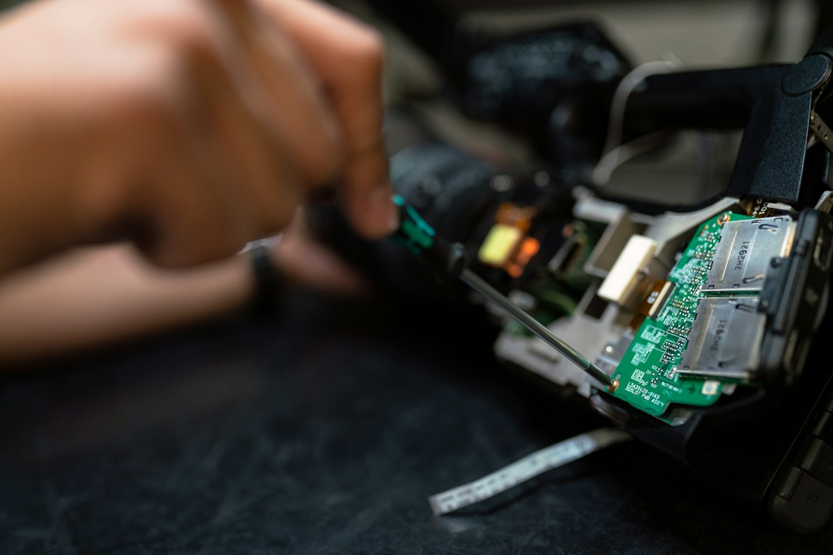
Comparison of 3 PCBA Outgoing Quality Control (OQC) Testing Methods
| Evaluation Criterion | Manual Wire-Harness Plugging & Laptop Flashing | Basic Mechanical Acrylic Jig Without Automated Measurement PCB | DeviceLab Turnkey Automated FCT Pogo-Pin Test Station |
|---|---|---|---|
| Cycle Time to Flash & Test 01 PCBA Unit | 10 – 15 minutes / board | 3 – 5 minutes / board (operator still flips toggle switches and reads multimeters manually) | 10 – 25 seconds / board (100% automated single-lever sequence) |
| Protection Against Solder-Bridge Power Shorts | High risk of IC burnout or trace vaporization when applying 24VDC directly | No automated cold-resistance check prior to power application | Automated cold rail impedance verification + 100μs electronic over-current trip before main power relay closure |
| Per-Board QC Data Traceability & Serialization | Handwritten paper tallies; impossible to audit during warranty claims | No automated measurement logging | Logs 100% of measured voltages/currents tied to MCU Unique ID + prints serialized QR barcode label |
Order Custom FCT Pogo-Pin Test Jigs & Turnkey Mass-Production PCBA at DeviceLab
Preparing to scale your electronic board into production batches of hundreds or tens of thousands of units and need an automated FCT Test Fixture that flashes firmware, verifies 100% of I/O functionality, and prints QR traceability labels? Send your Gerber files and functional test requirements to DeviceLab's R&D team for a turnkey quotation.
Field Engineering Frequently Asked Questions (Technical FAQ & B2B2B Partnership)
❓ What is an Electronic Functional Circuit Test Fixture (FCT / Bed-of-Nails Pogo-Pin Test Jig) and why is it mandatory for mass-production PCBA manufacturing?
An Electronic Functional Circuit Test Fixture (FCT / Bed-of-Nails Pogo-Pin Test Jig) is a custom-engineered mechatronic Automated Test Equipment (ATE) station that uses an array of spring-loaded contact probes (Pogo Pins) and a mechanical toggle-clamp or pneumatic press to simultaneously connect dozens of copper Test Points on the bottom side of a freshly soldered PCBA to an automated measurement and switching motherboard. When manufacturing anywhere from 300 to 50,000+ boards, an FCT Test Jig automates power-rail short-circuit screening, high-speed firmware flashing, and 100% peripheral loopback verification (Analog 4–20mA, Digital I/O, RS485, CAN, Wi-Fi/BLE/4G RSSI) in just 10 to 25 seconds per board—replacing slow, error-prone 15-minute manual cable harness testing.
❓ What is the difference between ICT (In-Circuit Test) and FCT (Functional Circuit Test) in an SMT electronics production line?
ICT (In-Circuit Test) measures the passive electrical value of individual discrete components on an unpowered board (checking resistor Ohms, capacitor Farads, diode orientation, and solder opens/shorts) and typically requires a $100,000+ USD industrial flying-probe or vacuum ICT machine justified only for ultra-high volumes (>50,000 units). Conversely, FCT (Functional Circuit Test) powers up the Device Under Test (DUT), provisions production firmware, and simulates real-world sensor inputs and actuator loads to certify 100% end-to-end operational functionality before enclosure assembly. For production runs of 200 to 50,000 units in Vietnam, a DeviceLab FCT Test Jig with integrated Pre-Power Short-Circuit Impedance Screening delivers the highest ROI and defect coverage.
❓ How should a hardware engineer design PCB Test Points (Design for Testability — DFT) to ensure 100% reliable Pogo-Pin contact?
During the PCB Layout phase (Design for Testability — DFT), hardware engineers should enforce five golden rules: (1) Place 100% of Test Points (TP) on the Bottom Layer of the PCB so the fixture only requires a single-sided bottom probe plate, cutting mechanical fixture cost by 50% compared to a dual-sided clamshell jig; (2) Size every exposed copper Test Pad at Ø1.0mm to Ø1.5mm diameter (with Solder Mask opening 1:1 and zero silkscreen overlap); (3) Maintain a minimum center-to-center pitch of >=2.0mm to 2.54mm (100 mil) between adjacent test points so rugged, high-current P100/P75 probes can be used; (4) Keep test points at least 3.0mm away from board edges and tall bottom-side SMD components; and (5) Include three asymmetric Ø3.0mm non-plated mechanical Tooling Holes at the board corners for ±0.05mm alignment accuracy.
❓ Which Pogo-Pin plunger tip geometry (Crown, Serrated, Spear, or Cup tip) provides the best electrical contact without damaging the PCB?
Selecting the proper spring-probe plunger tip style depends on the target landing structure on the PCBA: (1) 4-Point Crown Tip or 9-Point Serrated Waffle Tip (Style B or Q): optimal for flat HASL or ENIG-finished copper Test Pads and trimmed through-hole component leads, because the sharp micro-ridges bite cleanly through invisible no-clean rosin flux residue left after reflow soldering without skidding off the pad; (2) 30°/60° Conical Spear Tip (Style A): used exclusively for probing un-tented plated through-hole vias; and (3) Concave Cup or Spherical Tip (Style D or F): used for contacting gold-plated male connector pins or delicate conductive pads where surface indentation must be avoided.
❓ Can a DeviceLab FCT Test Jig automatically flash MCU firmware, lock readout protection, print QR Serial/MAC labels, and upload QC logs to the Cloud?
Yes—all executed hands-free in a single lever stroke. The moment the QC operator seats the PCBA onto the alignment pins and pulls down the Toggle Clamp: Step 1, the motherboard verifies that 24V, 5V, and 3.3V rails have zero solder-bridge shorts to GND within 0.5 seconds; Step 2, solid-state relays apply current-limited power and trigger an isolated high-speed programmer (SWD ST-Link / J-Link / CMSIS-DAP / ESP-Prog) to flash the production binary, inject calibration constants, and enable Readout Protection (RDP Level 1/2); Step 3, the fixture executes full I/O, RS485, 4–20mA, and RF loopback tests while reading the silicon Unique ID / MAC address; Step 4, upon 100% PASS, the host PC/Raspberry Pi automatically commands a Zebra/Godex thermal transfer printer to print a tamper-proof QR serial label and pushes the complete JSON/CSV test report to your Cloud QC database.
❓ What is the typical lead time and cost to engineer and fabricate a turnkey FCT Pogo-Pin Test Jig at DeviceLab?
DeviceLab designs, CNC-machines, wires, and programs a complete turnkey FCT Test Fixture—including precision CNC-milled ESD Antistatic Bakelite/POM carrier plates, gold-plated Receptacle + Plunger Pogo Pins, the internal measurement/switching PCB, and automated Pass/Fail test runner software—within 2 to 3 weeks. For clients engaging DeviceLab for Custom PCB Design or Turnkey PCBA Mass Production, our engineers build DFT testpads directly into the layout from Day 1, substantially reducing fixture fabrication cost and guaranteeing zero-defect batch deliveries.
Related Technical Articles & Engineering Guides
Deepen your engineering knowledge with practical guides from DeviceLab engineers:


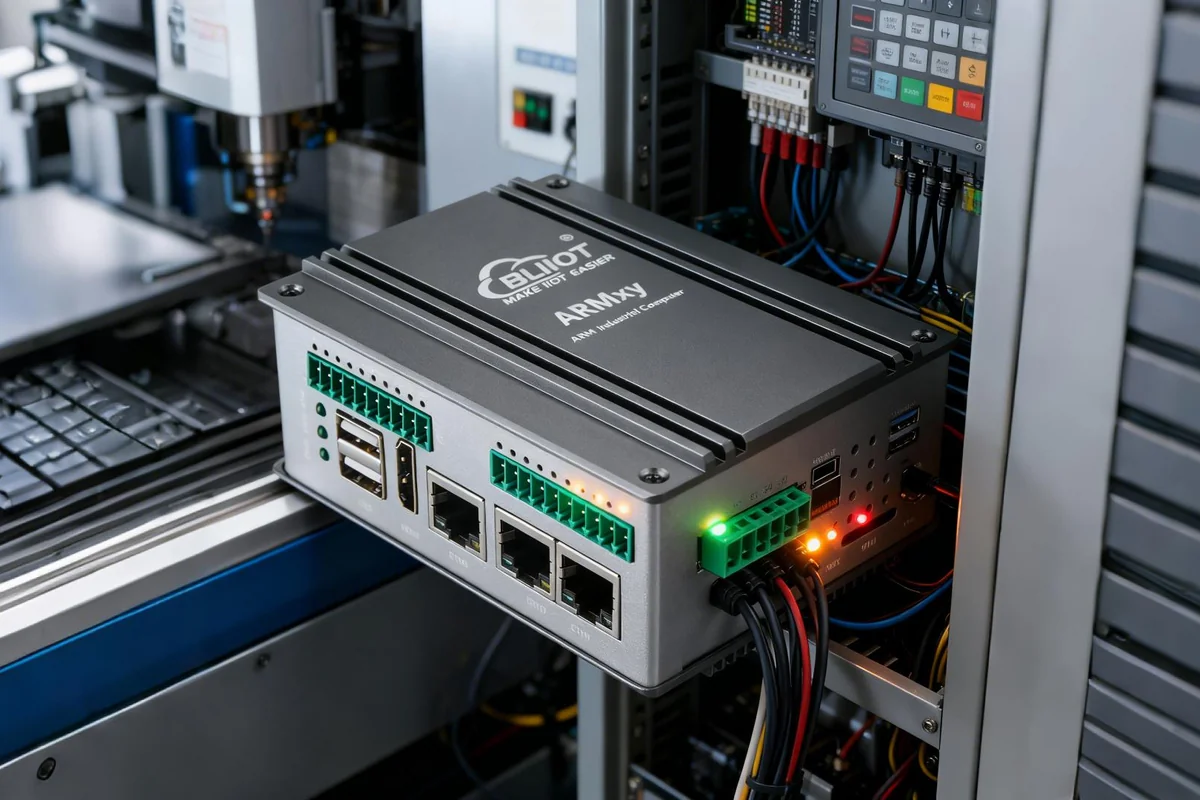
Recommended Industrial IoT Hardware & OEM Solutions
Standardized industrial-grade devices engineered and mass-produced by DeviceLab Vietnam:
Need custom hardware design or embedded device engineering?
You do not need a complete schematic. Describe your functional specifications, target application, and power/size/connectivity constraints.
DeviceLab helps define engineering scope from architecture to functional prototype.