
Turnkey Manufacturing & QC Engineering for Industrial IoT
End-to-end OEM/ODM hardware manufacturing tailored for industrial machinery builders, Circular 10 environmental SI contractors, and IoT software providers. From rigorous DFM/DFT optimization and genuine component sourcing to 100% automated pogo-pin FCT test jigs and 72-hour thermal stress burn-in validation.
Real Workshop Facilities & SMT Electronics Manufacturing Lines
Unlike pure trading brokers, DeviceLab directly operates automated SMT pick-and-place lines, reflow soldering tunnels, custom FCT test fixtures, and cable harness processing equipment in Vietnam.

Technicians Operating Automated SMT Lines
DeviceLab technicians directly monitor high-speed pick-and-place machinery, feeder trays, and multi-board panel alignment.

Visual Inspection & Antistatic Batch Packaging
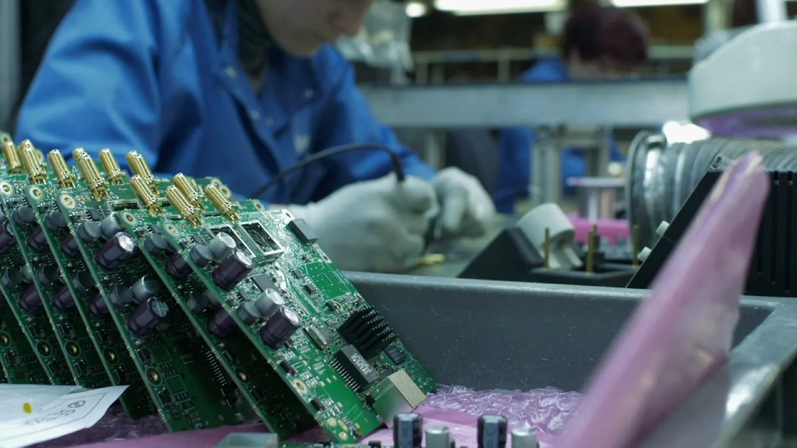
100% visual inspection of solder joints and antistatic bubble wrap packaging on ESD-safe assembly workbenches.

Multi-Zone Reflow Soldering Oven
Multi-zone convection thermal profiling oven with real-time temperature curve monitoring ensures optimal solder joint reliability.

Cleanroom Facility & Optical AOI Inspection
Engineers operating under controlled cleanroom environment with inline Automated Optical Inspection (AOI) machines.

High-Density BGA & RAM Kingston PCBA
Real-world high-speed multi-layer industrial IoT controller designed and assembled by DeviceLab with impedance-matched differential traces.

Automated Wire Stripping & Harness Crimping
Dedicated industrial stripping and terminal crimping machinery ensuring high-reliability cable harness fabrication for control panels.
4 Layers of Rigorous Hardware Quality Assurance
From incoming silicon verification to continuous burn-in stress testing, every production step is governed by documented Standard Operating Procedures (SOPs) ensuring zero field defects.
Layer 1: Incoming Materials
IQC – Incoming Quality Control
Zero counterfeit silicon policy. 100% active parts sourced from authorized global tier-1 supply chains with full CO/CQ documentation.
- Manufacturer Part Number (MPN), date-code, and Moisture Sensitivity Level (MSL) verification.
- Raw PCB fabrication inspection: FR-4 High-TG170, ENIG gold plating, and flying probe continuity tests.
- Sample LCR impedance testing on passive components (inductors, TVS diodes, capacitors).
Layer 2: SMT Assembly & Inspection
IPQC – In-Process SMT Assembly
Automated pick-and-place lines operating under IPC-A-610 Class 2/3 manufacturing standards with optical and radiological inspection.
- Solder Paste Inspection (SPI) ensuring uniform paste deposition across fine-pitch pads.
- Automated Optical Inspection (AOI) verifying 100% of surface-mount components post-reflow.
- X-Ray inspection for hidden solder joints on BGA, QFN, and 4G wireless module land grids.
- Optional protective conformal coating against humidity, salt fog, and industrial chemical fumes.
Layer 3: Automated Testing Jigs
FCT – Functional Circuit Test
Custom-engineered pogo-pin test fixtures running automated bring-up scripts on 100% of manufactured boards before packaging.
- Automated power rail profiling: input reverse polarity, buck converter ripple, quiescent current.
- Automated firmware flashing with hardware root-of-trust encryption key provisioning.
- Loopback testing on isolated RS485, RS232, DI/DO optocouplers, ADC 4-20mA, and RTC battery.
- Live RF test: 4G LTE Cat 1 network attach, MQTT packet dispatch, and GPS lock latency.
Layer 4: Burn-In Stress & Outgoing QC
OQC & Thermal Burn-In Stress Testing
Simulating years of field operation in elevated temperature stress chambers to purge infant silicon mortality before final dispatch.
- 48 to 72 hours continuous full-load burn-in in controlled thermal stress chambers.
- Accelerated power cycling test (>200 on/off cuts) verifying flash file system integrity and watchdog recovery.
- Final enclosure fitment, laser-engraved serial QR code, QC Pass seal, and inspection report archiving.
From Prototype to 1,000+ Production Units
Structured engineering milestones designed to eliminate financial and technical risks for B2B partners. You validate in the field before committing capital to mass production.
DFM & Functional Prototype
2 – 4 Weeks · 1–5 unitsSchematic capture, PCB layout optimized for manufacturing (DFM), bench assembly, and initial firmware bring-up in our Hanoi laboratory.
Pre-Compliance & Lab Validation
1 – 2 Weeks · Bench TestingComprehensive bench testing: DSO signal integrity, logic protocol decoding, ESD gun testing (±15kV), and surge transient validation.
Pilot Field Deployment
30 – 60 Days · 20–50 unitsMounting pilot hardware directly on partner machinery or environmental monitoring stations. Real-world validation before frozen BOM release.
Turnkey OEM Mass Production
4 – 6 Weeks · 100–1,000+ unitsVolume SMT assembly, automated pogo-pin FCT fixture testing, 72h thermal burn-in, custom private-label branding, and turnkey boxed delivery.
 ⚡ 100% Automated FCT Pogo-Pin Test Jigs
Custom Pogo-Pin Test Fixtures Built for Every Single Production Batch
Manual multimeter probing cannot scale beyond a few dozen prototypes. For every OEM hardware model, DeviceLab engineers a dedicated Pogo-Pin Test Fixture that mates with precision test points laid out during PCB design.
- Zero-Human-Error Flashing: Automated bootloader flashing, firmware payload verification, and factory calibration offset programming in under 30 seconds.
- 100% Peripheral Loopback: Active validation of dual isolated RS485 transceivers, optocoupled inputs, relay contactors, micro-SD cards, and RTC battery life.
- RF Transmission Verification: Cellular modem attach, SIM card handshake, RSSI signal margin test, and test payload transmission to our cloud server.
- Serial & Traceability Log: Only boards passing all automated tests receive an encrypted serial ID and digital inspection certificate archived in our ERP.
Laboratory Test Instrumentation & Prototyping Tools
DeviceLab invests continuously in advanced electronic measurement equipment to validate physical-layer signal integrity, protocol adherence, and electromagnetic pre-compliance.
Digital Storage Oscilloscopes (DSO)
High-bandwidth multi-channel digital storage oscilloscopes measuring high-speed bus rise times, power rail ripple, and clock jitter.
16-Channel Logic Analyzers
Real-time multi-channel protocol analysis decoding SPI, I2C, UART, Modbus RTU, and CAN-bus industrial packets.
ESD Simulator Gun (IEC 61000-4-2)
Electrostatic discharge testing up to ±8kV contact and ±15kV air discharge on all external ports and metallic enclosures.
Surge & Fast Transient Simulator
Evaluating circuit protection on RS485 and 24VDC industrial power ports against high-energy lightning surges (IEC 61000-4-5).
Programmable DC Electronic Loads
Multi-channel constant current/voltage/power profiling evaluating thermal dissipation and overcurrent trip thresholds.
Thermal Aging & Burn-In Chambers
Environmental burn-in chambers (-40°C to +85°C) running round-the-clock stress tests on production batches.
DeviceLab vs Alternative Approaches
Compare the turnkey hardware partnership model against in-house engineering, raw SMT assembly, or freelance developers.
| Criteria | In-House Hardware Team | Raw SMT Assemblers | ★ DeviceLab Turnkey Partner |
|---|---|---|---|
| Fixed Overhead & Payroll | High ($5,000–$10,000/mo) for hardware, layout, and firmware engineers. | Low fixed cost, but you manage entire BOM, procurement, and testing. | Zero payroll overhead. Pay per batch milestone with shared NRE incentives. |
| Functional Testing (FCT) | Manual bench testing; lack of automated pogo-pin tooling. | None. Only visual AOI solder inspection; zero functional validation. | 100% automated pogo-pin test jig built specifically for your board model. |
| Reliability & Burn-In | Rarely have thermal stress chambers; high field failure risk in early batches. | Not provided. | 72-hour continuous thermal burn-in stress testing purging infant mortality. |
| Time to Market | 6 to 12 months for hiring, tool setup, and prototype iteration. | Fast assembly, but slow integration and debugging. | 6 to 10 weeks from functional specification to bench-verified field pilot. |
| Component EOL & Supply Chain | Vulnerable to silicon obsolescence and stockouts. | Only mounts what client supplies; no lifecycle guidance. | Multi-source footprint design + Tier-1 distributor relationships with 10+ year MCU roadmap. |
B2B Commitments & Brand Protection
DeviceLab operates as an invisible engineering and manufacturing backend. We exist to empower our partners to win their markets under their own brand.
🏷️ 100% White-Label Delivery
Your brand on the enclosure, laser-etched nameplates, packaging, documentation, and companion IoT web/mobile software.
🤝 Binding Non-Compete Guarantee
We sign legal agreements never to approach, quote, or sell directly to your end clients. We exclusively serve solution partners.
🔒 Strict Mutual NDA Protection
Non-disclosure agreements executed before receiving requirements. All proprietary firmware and schemas remain strictly protected.
🛠️ Direct Senior Engineering Access
Direct communication channel with lead hardware and firmware engineers throughout production and field lifecycle.
Frequently Asked Questions About Manufacturing & QC
Key operational and commercial questions answered for engineering directors and procurement managers.
What is the Minimum Order Quantity (MOQ) for OEM/ODM hardware batches?
How does DeviceLab ensure 100% functional reliability for manufactured boards?
Does DeviceLab provide complete white-label customization and brand protection?
How does DeviceLab mitigate component obsolescence and supply chain risks?
What technical documentation and warranty support are provided with production batches?
Ready to Manufacture Field-Reliable Hardware Under Your Brand?
Schedule a direct engineering consultation and in-person laboratory walkthrough in Hanoi. We analyze your DFM requirements, component BOM budget, and production schedule within 24 to 48 hours.