Skip to content

Engineering Partner · Hardware · Embedded · Prototype to Production

Custom Electronic Device Development

From functional requirements and concept specifications to bench prototypes and turnkey commercial mass manufacturing.

DeviceLab partners with OEMs, enterprises, and tech startups worldwide as an end-to-end R&D Engineering Partner. You have a breakthrough product concept, a challenging field monitoring requirement, or need specialized connected hardware unavailable on the commercial market. You do not need preexisting schematics or silicon selection experience. Describe your functional requirements in plain language—our engineers will formulate the system architecture, capture hardware schematics, code low-level firmware, assemble bench prototypes, and prepare documentation for volume production with optimized BOM economics.

✓ Protected by Mutual NDA  ·  ✓ COTS vs. OEM vs. Custom Evaluation  ·  ✓ Working Hardware Delivery

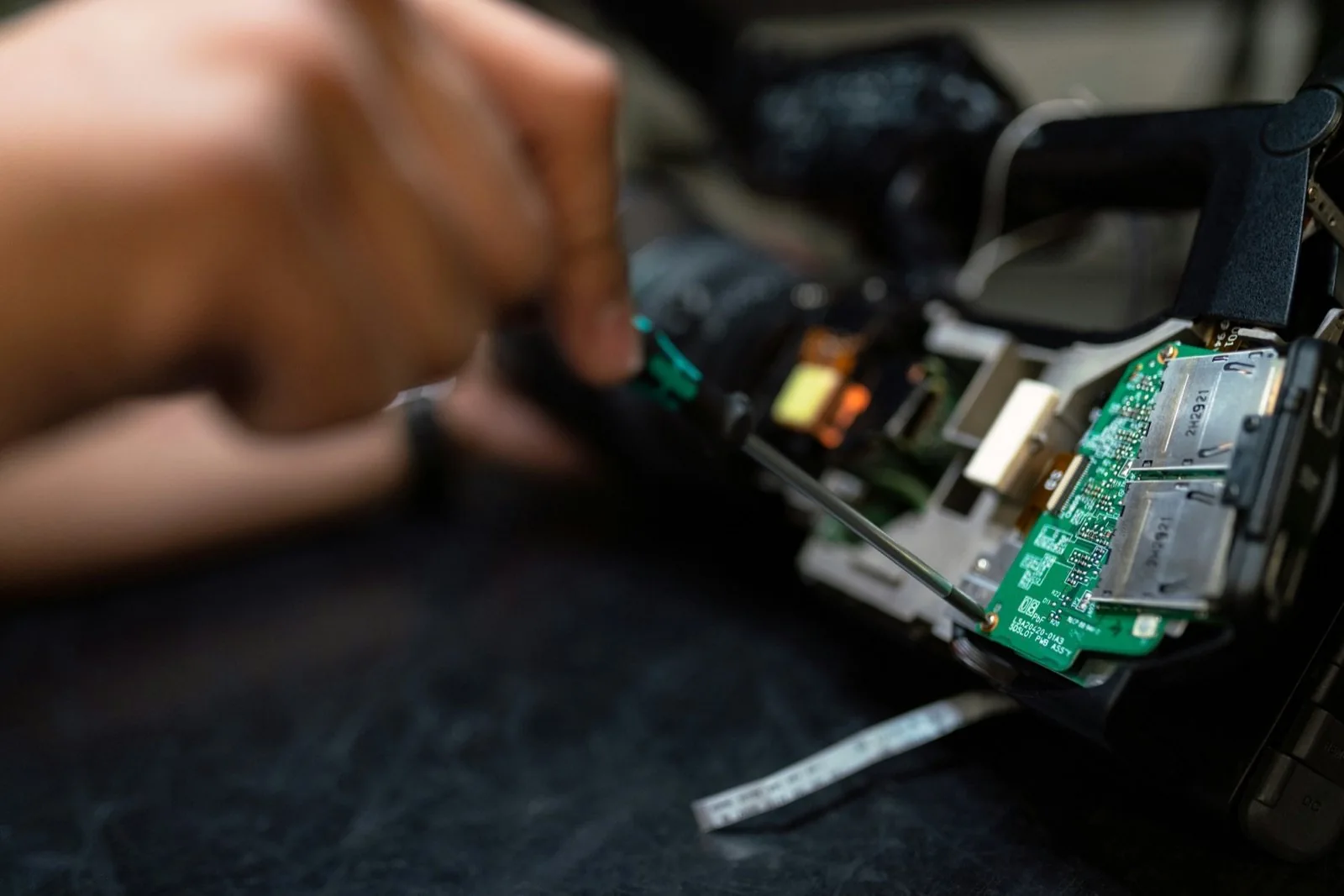
DeviceLab senior engineers testing prototype electronic boards on laboratory benches

What is Custom Electronic Device Engineering?

Custom Electronic Device Engineering is the disciplined process of researching, designing, and fabricating specialized electronic hardware tailored to precise operational criteria that off-the-shelf commercial equipment cannot satisfy. This encompasses 4 deeply integrated engineering disciplines: Hardware & Multi-layer PCBA Design, Embedded Firmware & OS (C/C++, FreeRTOS, Embedded Linux), Mechanical Enclosure CAD, and Cloud/Server Fleet Integration. The ultimate objective is a ruggedized product operating reliably 24/7 in demanding field environments, de-risked against component obsolescence, and optimized for mass manufacturing.

Industry Realities & Pitfalls

4 Engineering Traps That Derail Hardware Projects Before Market Launch

In our experience co-engineering products with technology founders and enterprise engineering leads, hardware projects rarely stall due to lack of capital. They stall due to critical architectural traps:

1. The "Hobbyist Breadboard" Trap

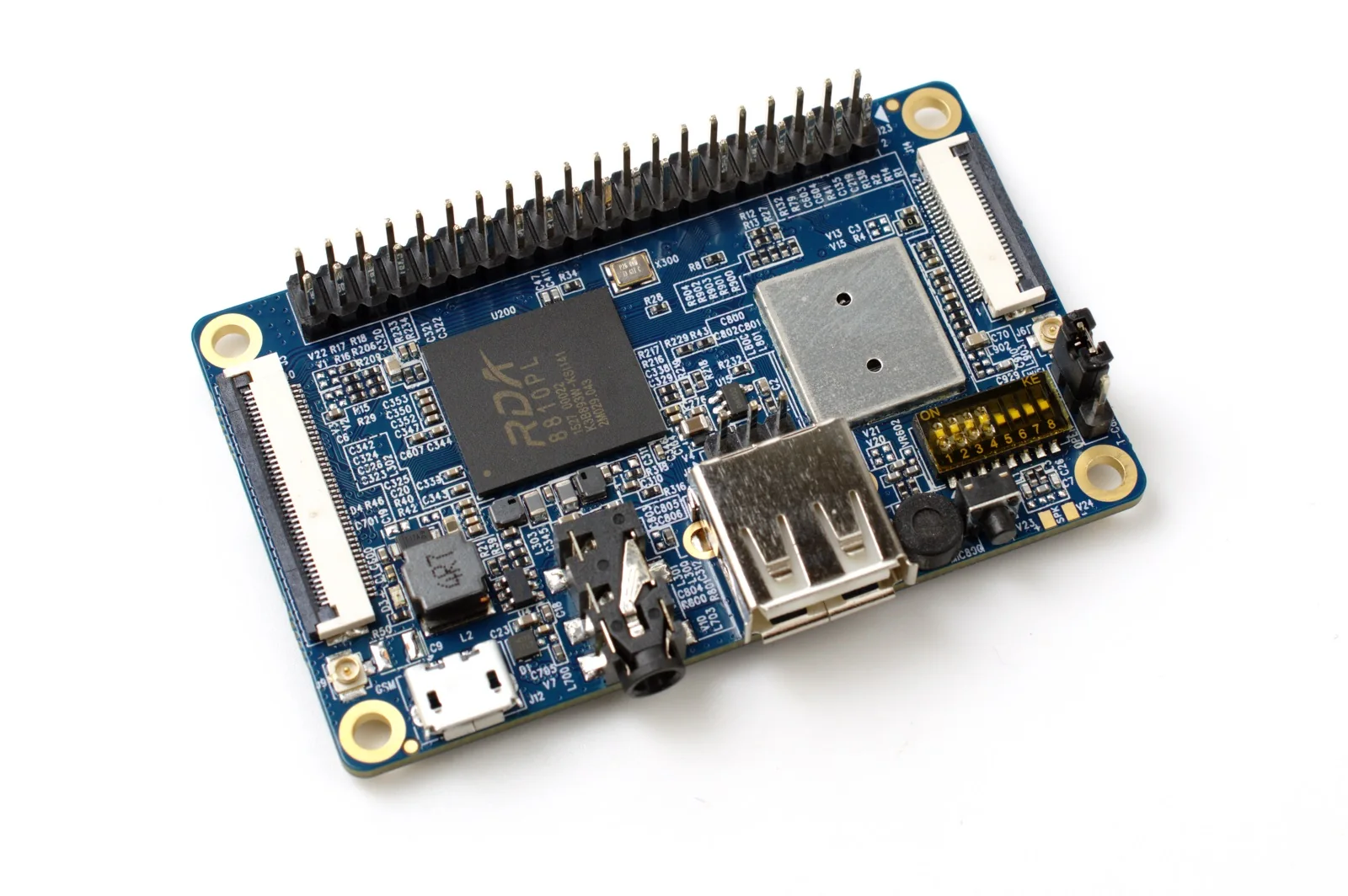
Assembling a proof-of-concept on Arduino or Raspberry Pi dev boards is quick on an air-conditioned desk. But when moved into harsh field conditions, it suffers brownouts from power rail transients, exceeds enclosure dimensions, fails industrial thermal ratings, and carries an inflated BOM cost unviable for commercial sale.
2. The "Drafting-Only Layout" Trap

Hiring a freelancer solely to route PCB traces from a basic schematic yields Gerber files, but no accountability. Once SMT assembled, no one writes low-level drivers, the board suffers high-speed clock noise or ground bounce, and nobody assumes responsibility for fixing the hardware.

3. The "Missing Remote OTA Lifecycle" Trap

Deploying hundreds of connected units without fail-safe Over-the-Air (OTA) firmware pipelines or dual-bank rollback mechanisms creates an operational nightmare. A minor firmware bug forces expensive dispatch of field technicians across regions to manually re-flash boards.

4. The "Single-Source Obsolescence (EOL)" Trap

Selecting niche silicon without validating manufacturer product lifecycle status. Just as prototypes achieve sign-off for volume production, the primary microcontroller enters allocation with 40-week lead times, forcing an expensive, multi-month board redesign from scratch.

DeviceLab engineers specifically to neutralize these pitfalls: We do not treat hardware as an isolated circuit board. We engineer complete commercial products—integrating DFM, component resilience, and field lifecycle maintenance from day one.

Target Audience

Who We Partner With

Every organization approaches hardware development with distinct technical constraints. We architect solutions calibrated to your exact business model.

Startups & Hardware Innovators

The Context: Promising product concept or early bench demo on hobby kits. Lacking an internal hardware R&D bench, they risk misallocating capital on unviable PCB revisions.

DeviceLab Solution: Architectural guidance, cost-optimized silicon selection, compact industrial PCBA layout, complete enclosed prototypes, and BOM modeling ready for investor funding and market trials.

Industrial Plants & Manufacturers

The Context: Need real-time monitoring of machinery, electrical power, pressure, or temperature. Foreign commercial equipment is cost-prohibitive and incompatible with proprietary in-house software.

DeviceLab Solution: Rugged Industrial IoT Gateways, isolated DIN-rail controllers, multi-port RS485 Modbus RTU, wide-temperature resilience, and noise immunity for dusty switchgear cabinets.

Software & Cloud SaaS Houses

The Context: World-class Backend, Web, Mobile App, and AI competencies; need to deploy physical devices into the field (touch kiosks, AI vision cameras, card readers, sensors) without the overhead of an in-house hardware team.

DeviceLab Solution: Turnkey Hardware + Firmware + Connectivity layers, providing clean REST/MQTT schemas that integrate into your existing cloud platform as plug-and-play appliances.

System Integrators (SI) & Contractors

The Context: Commissioning IP audio, access control, and smart campus infrastructure. Major global brands enforce vendor lock-in or charge exorbitant pricing that erodes contracting margins.

DeviceLab Solution: Turnkey white-label or OEM/ODM hardware platforms, full protocol transparency, rapid lead times, direct field technical support, and long-term hardware warranties.

Strategic Execution Paths

Evaluating COTS Customization vs. OEM/ODM vs. Full Custom Hardware

A skilled engineering partner identifies the lowest-risk, most cost-effective path to field deployment—never forcing an expensive custom design when an alternative delivers superior ROI.

Evaluation Parameter 1. COTS Customization 2. OEM / SOM Platform 3. Full Custom Device
Time-to-Prototype Ultra-fast (2–4 weeks) Fast (1–2 months) Rigorous (2–4 months)
Upfront NRE Investment Minimal / None Low to Moderate Full project engineering
Unit Cost at Volume High (fixed vendor margins) Moderate Optimized BOM (Lowest)
Hardware IP Ownership None Partial (Carrier & Firmware) 100% Full IP (Schematics + Code)
Enclosure Customization Fixed vendor housing Custom branding/faceplate 100% tailored to mechanical space
Ideal Production Scale Under 50–100 units 100 to 1,000 units 500 to tens of thousands
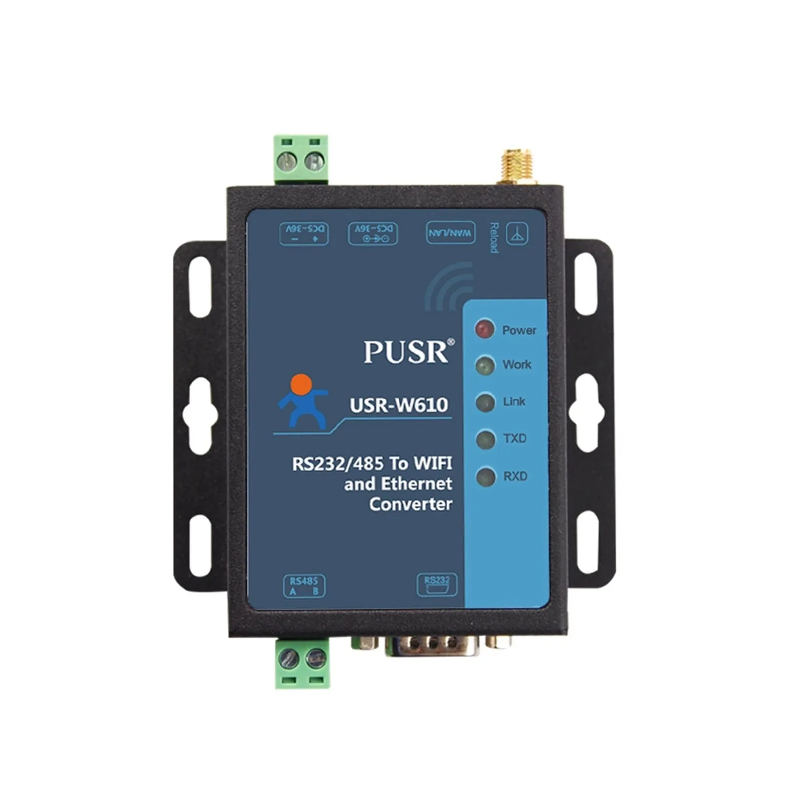
Commercial IoT gateway and modules for rapid customization

01 · Rapid Deployment

COTS Customization

When an existing industrial device satisfies 85%+ of functional needs, we write custom firmware or attach daughterboards to integrate it into your platform.

  • Immediate market launch required
  • No deep hardware modifications needed
  • Early stage, low initial deployment volume
System on Module SOM embedded boards for rapid OEM customization

02 · Platform Acceleration

OEM / ODM Platform Customization

Utilizing pre-certified System-on-Modules (SOM / Compute Modules), designing only custom carrier boards and specialized firmware under your private brand.

  • Cuts CPU core R&D schedule by 50%
  • Proprietary branding and tailored I/O
  • Robust platform for mid-to-high commercial volume
Custom engineered multi-layer circuit boards

03 · Proprietary Engineering

Full Custom Device Engineering

Schematic capture, multi-layer high-speed PCB routing, low-level firmware, and custom mechanical enclosures when bound by strict size, battery, or unit BOM targets.

  • Strict mechanical or battery longevity constraints
  • 100% Intellectual Property ownership
  • Maximum unit BOM cost optimization at scale

Unified Competency

Integrated Technical Disciplines in Every Hardware Product

A modern connected device integrates precision electronics, low-level embedded software, telecommunications, and cloud platforms. We master the complete chain so you avoid fragmented outsourcing:

1. Hardware Engineering & Multi-Layer PCB

From low-power 32-bit MCUs (STM32, ESP32, NXP, Renesas) to Linux-capable MPUs/SoCs (Rockchip, Allwinner, NXP i.MX). Wide-range industrial power designs (9–36VDC), reverse-polarity protection, high-energy TVS surge clamps. High-speed 4–8 layer PCB layout with controlled impedance (USB, Ethernet, HDMI) and pre-compliance EMC/EMI mitigation.

2. Firmware & Embedded Operating Systems

Firmware development in bare-metal C/C++ or Real-Time Operating Systems (FreeRTOS, Zephyr) for deterministic sub-millisecond execution. Hardened Embedded Linux built with Yocto / Buildroot booting in under 5 seconds. Secure dual-bank A/B fail-safe Over-the-Air (OTA) bootloaders with automatic rollback.

3. Industrial Telecommunications & Fieldbus

Wired fieldbuses: RS485 Modbus RTU with 2.5kV galvanic optical isolation, CAN-bus, and gigabit Ethernet PoE. Wireless connectivity: 4G LTE Cat-1/Cat-4, NB-IoT, low-power LoRaWAN, Wi-Fi 6, and BLE Mesh. Standardized messaging via encrypted MQTT over TLS and HTTPS REST APIs.

4. Edge AI & Embedded Computer Vision

Integrating processors with dedicated Neural Processing Units (NPUs from 1.0 to 6.0 TOPS) to execute neural networks on-device (Edge AI). Real-time facial recognition attendance, Automatic Number Plate Recognition (ANPR), and automated optical inspection (QC) running locally under 0.3s without cloud latency.

5. Mechanical CAD & Protective Enclosures

Rapid enclosure prototyping via industrial SLA/SLS 3D printing for immediate mechanical verification with PCBA samples. Custom CNC-milled aluminum extrusions with passive thermal dissipation; fire-retardant ABS/PC injection-molded housings rated IP65/IP67 for outdoor weatherproofing; standard DIN-rail mounts.

6. Cloud Telemetry & Device Fleet Management

Managing the operational lifecycle of distributed devices. Responsive Web Dashboards displaying online status (heartbeat), remote parameter reconfiguration, regional batch OTA upgrades, immediate Telegram/SMS alarm notifications, and diagnostic error logging.

Product Showcase

Hardware Product Categories We Engineer

From rugged switchgear controllers to high-throughput smart vision terminals:

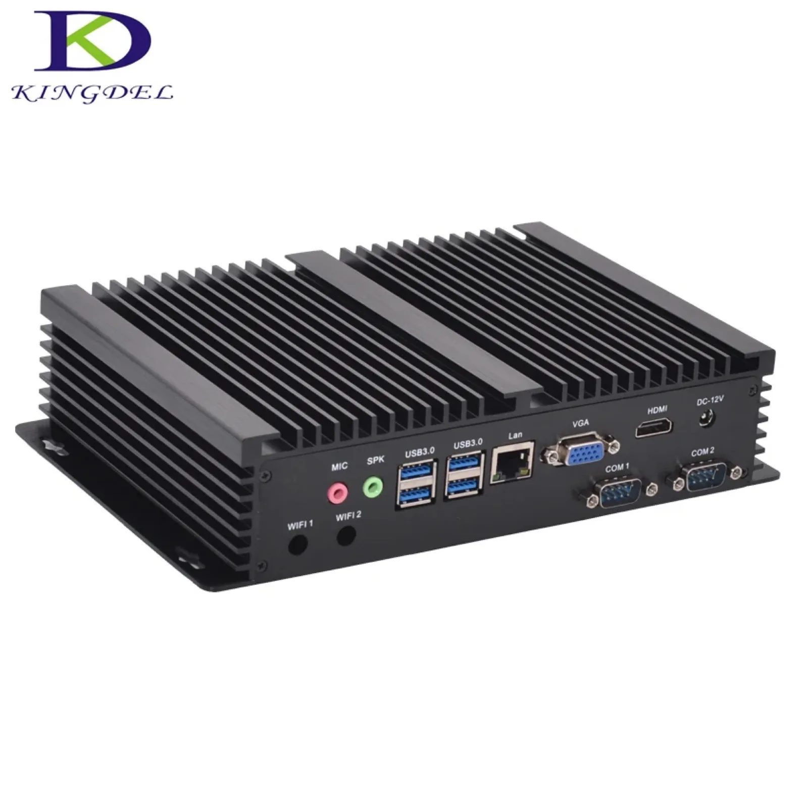
Industrial IoT Gateway for data acquisition and telemetry

Industrial IoT Gateways

Central gateway appliances polling Modbus registers across machinery, sub-meters, and environmental sensors, preprocessing telemetry and dispatching data via 4G/Ethernet.

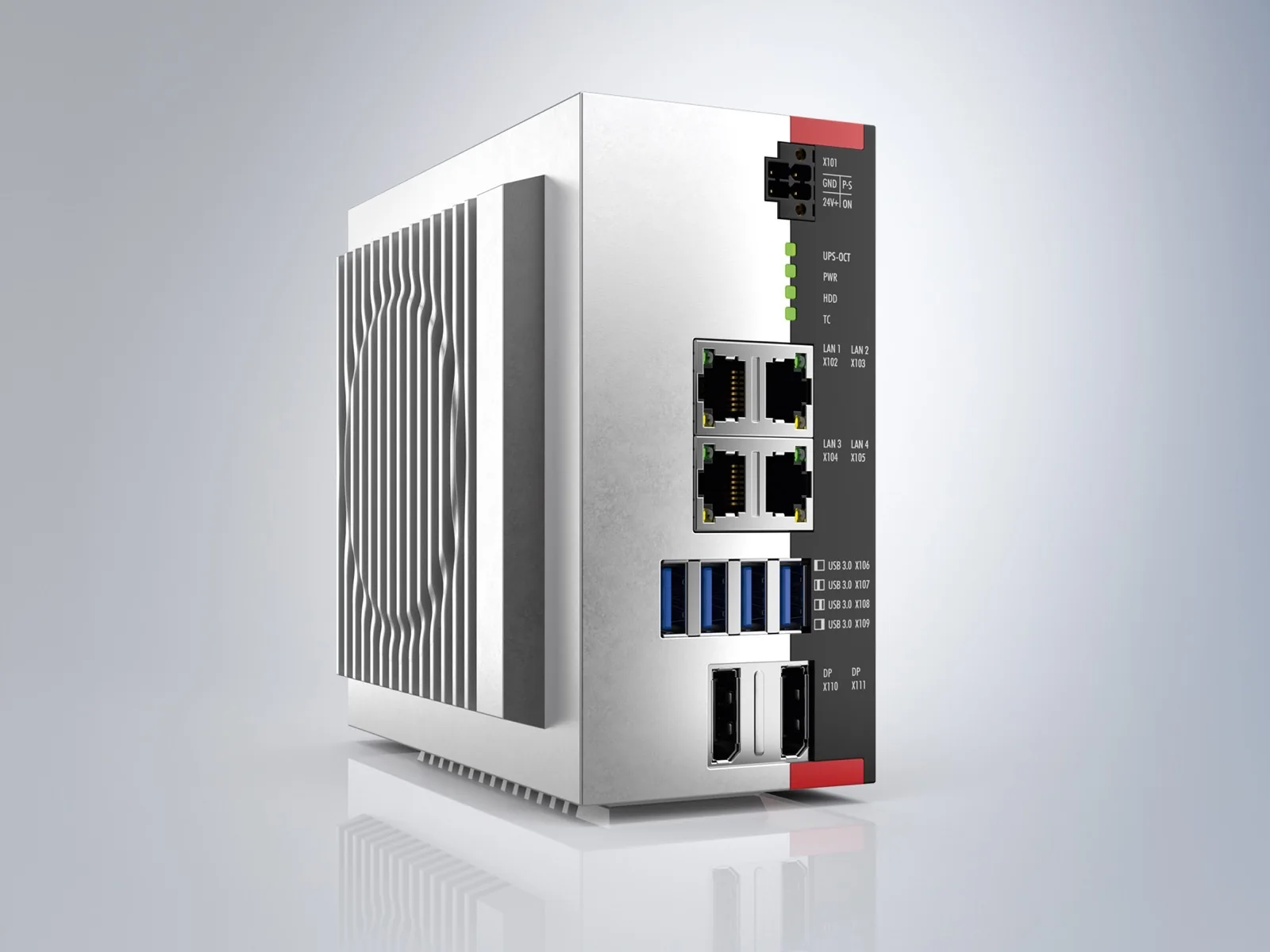
Rugged DIN-rail industrial controller

Industrial Controllers

Specialized controllers for industrial automation, pump stations, and switchboards. Digital/Analog I/O (DI/AI), high-current relay outputs (DO), engineered for continuous vibration and heat.

Industrial Edge AI computing box

Edge AI Boxes

Rugged fanless embedded computers with integrated NPUs for localized computer vision, access control, and conveyor quality inspection.

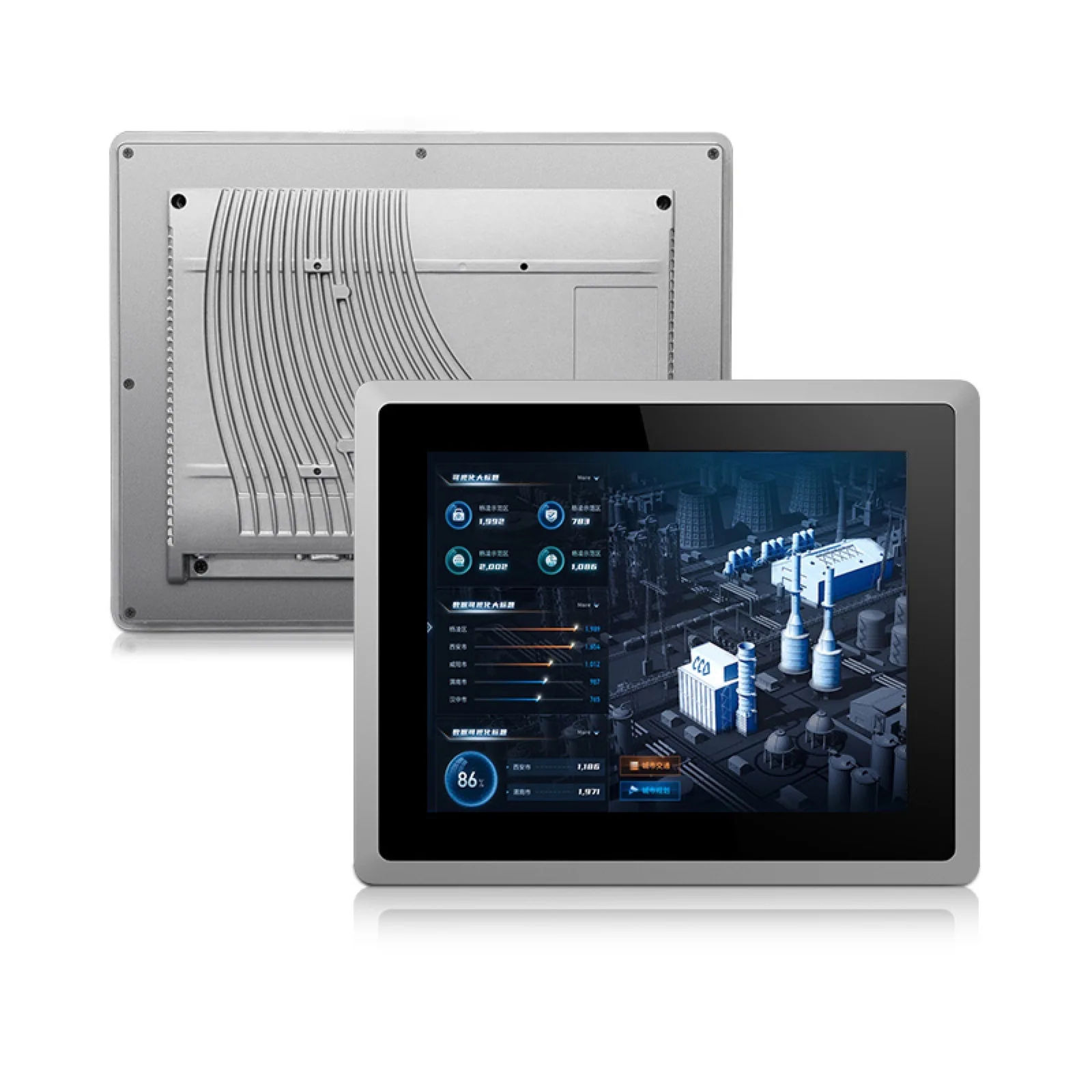
Smart interactive terminal and HMI

Smart Terminals & Interactive Kiosks

HMI touch interfaces, QR/barcode scanners, and NFC readers for smart attendance, self-service kiosks, and machine operational consoles.

Precision sensor and telemetry device

Wireless Sensors & Monitoring Nodes

Environmental sensors, gas monitors, vibration nodes, and level indicators operating for years on internal batteries via LoRaWAN or NB-IoT.

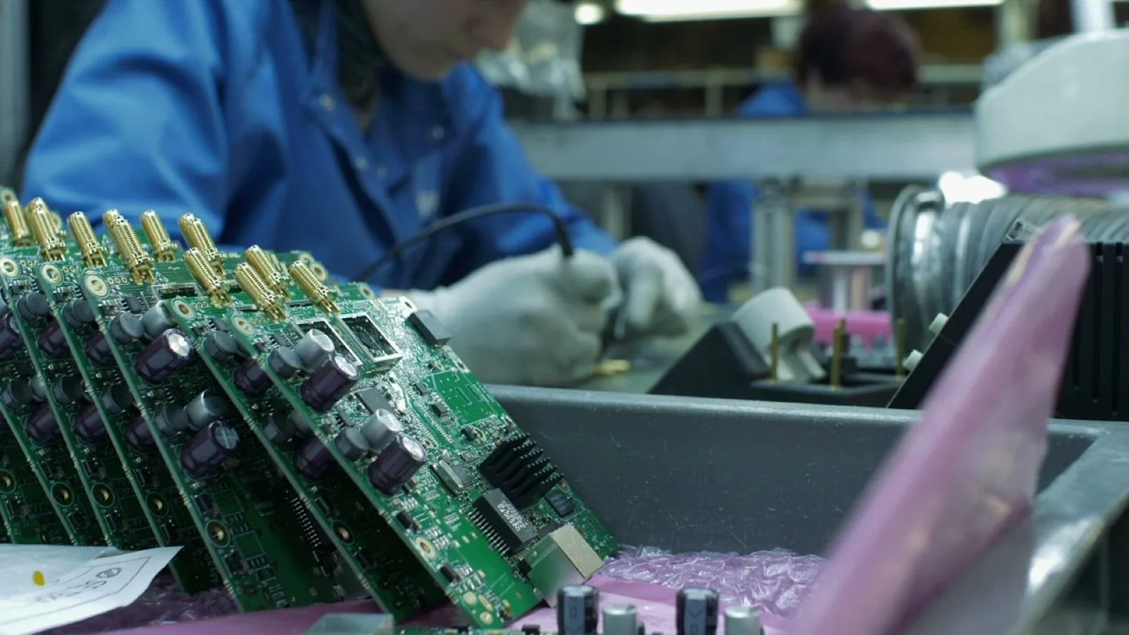
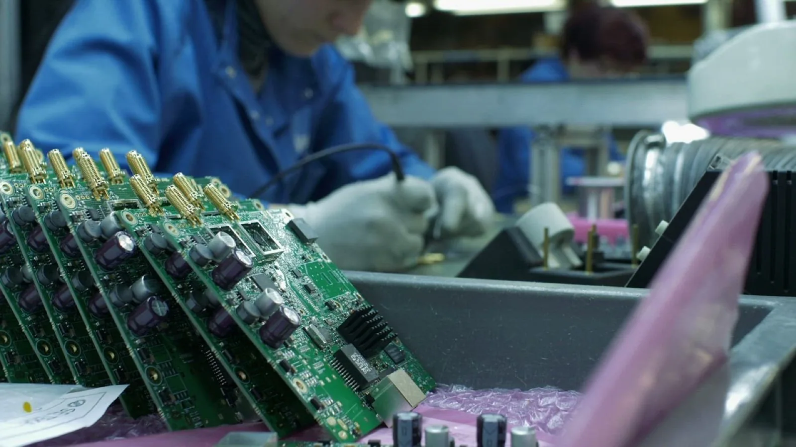
Precision SMT electronics assembly line

Custom Specialty Electronics

Proprietary electronic devices tailored to unique operational criteria: zoned IP audio endpoints, custom medical equipment boards, or specialized educational hardware.

R&D Methodology

7-Stage Engineering Lifecycle: Concept to Mass Production

Hardware mistakes made in early stages compound exponentially in production. Our disciplined engineering lifecycle de-risks development at each milestone:

01

Stage 1: Briefing, Mutual NDA & Feasibility (1–3 Days)

Reviewing functional requirements, physical environment, and unit budget targets. Mutual NDA execution. Technical feasibility analysis evaluating COTS, OEM, or Custom pathways.

02

Stage 2: Architecture & Target BOM Costing (1–2 Weeks)

Formulating system block diagrams, delineating hardware/firmware boundaries, selecting primary silicon with long-term lifecycle availability, and preliminary volume BOM modeling.

03

Stage 3: Schematics & Multi-Layer PCB Layout (2–3 Weeks)

Capturing comprehensive schematics in Altium Designer, circuit simulation, impedance-controlled PCB routing, pre-compliance EMC/EMI mitigation, and DFM optimization.

04

Stage 4: Prototype PCBA Assembly & Board Support Package (1–2 Weeks)

High-precision SMT fabrication of prototype boards in our lab. Concurrently, embedded engineers develop Board Support Package (BSP) drivers, GPIO mappings, and peripheral testing routines.

05

Stage 5: Laboratory Instrumentation & Working Prototypes (1–2 Weeks)

Rigorous bench testing using oscilloscopes and logic analyzers: verifying power rail ripple under load, thermal profiling, flashing application firmware, and fitting custom enclosures.

06

Stage 6: Field Pilot Trials & Design Refinement (2–4 Weeks)

Deploying working prototypes into actual customer operating environments (plants, schools, cabinets). Analyzing telemetry logs, verifying noise immunity, and refining firmware/mechanics based on field empirical data.

07

Stage 7: Production Tooling & 100% IP Handover

Engineering automated test fixtures (FCT Jigs) for high-speed factory validation, preparing Standard Operating Procedures (SOP), and transferring complete design files and uncompiled code under 100% client ownership.

Guaranteed Ownership

Deliverables & 100% Intellectual Property (IP) Handover

We operate as your transparent engineering partner, avoiding vendor lock-in. Upon final sign-off, all technical assets are transferred to ensure your complete independence:

1. Working Hardware Prototypes

Fully assembled, bench-verified prototypes housed in custom enclosures, pre-flashed with firmware, ready for field trials or customer demonstrations.

2. Complete Hardware Design Package

Original Altium/KiCad schematic files, PCB layout files, symbol and footprint component libraries, and manufacturing Gerber, Drill, and Pick & Place archives.

3. Detailed Bill of Materials (BOM) & Sourcing

BOM identifying 100% exact manufacturer part numbers, verified suppliers, and approved global distributors (DigiKey, Mouser, LCSC, Arrow).

4. Firmware Source Code & Build Toolchains

Clean, documented source code with build instructions, toolchain configuration guides, and flashing procedures via SWD/JTAG and over-the-air (OTA).

5. Interface Control Document (ICD)

Formal specification detailing packet structures, Modbus register maps, MQTT JSON schemas, and error codes enabling immediate backend integration.

6. 100% Legal IP Transfer Covenant

You hold exclusive commercial and patent rights. DeviceLab guarantees absolute confidentiality and never shares designs with third parties.

Field Deployments

Proven Hardware Systems Operating Daily in the Field

See how DeviceLab engineers complex technical criteria into rugged, field-operating commercial platforms serving thousands of daily users:

View All Case Studies

Industrial IoT — Energy Monitoring & Plant Telemetry System

Connects transformers, digital power meters, sensors, and legacy machines into a unified monitoring platform. Tracks electrical load profiles, detects phase imbalances, and optimizes factory operational costs.

  • Industrial IoT
  • Modbus RS485
  • Energy SCADA
  • MQTT Gateway

Edge AI Box — Real-Time Computer Vision & On-Device Inference

Industrial edge computer equipped with onboard NPU hardware achieving sub-50ms local computer vision inference. Deployed for automated defect detection (QC) and workshop safety monitoring without internet dependency.

  • Edge AI
  • Computer Vision
  • NPU Hardware
  • Industrial PC

Technical Knowledge & Insights

Battle-tested insights from DeviceLab senior engineers: industrial noise immunity, fail-safe dual-bank OTA firmware, BOM cost optimization, and DFM standards for volume manufacturing:

View All Technical Articles →

Technical Clarifications

Frequently Asked Questions on Device Engineering

1. We only have a functional concept or specification brief without schematics. Can DeviceLab engineer the device?

Yes, absolutely. Over 70% of our clients engage DeviceLab at the functional brief or prototype concept stage. You do not need preexisting schematics or silicon selection experience. Our senior engineers translate your operational requirements into a formal hardware architecture, capture schematics, layout multi-layer PCBs, write firmware, assemble prototypes, and prepare documentation for mass manufacturing.

2. How much does custom electronic device development cost and how is it billed?

Non-Recurring Engineering (NRE) costs depend on three factors: functional complexity (basic sensor telemetry vs. high-speed Edge AI vision), operating environment (commercial indoor vs. rugged industrial EMC ratings), and delivery schedule. DeviceLab provides transparent, milestone-based, fixed-scope proposals with zero hidden fees and clear acceptance deliverables at each sprint.

3. What is the typical timeline to deliver a working hardware prototype?

For standard microcontroller-based IoT devices or control boards, timeline from technical freeze to fully assembled, bench-tested working prototypes is 4 to 8 weeks. For complex high-density platforms (multi-core Linux MPUs, multi-camera computer vision, custom injection mold tooling), development spans 8 to 16 weeks, including iterative field testing.

4. Who owns the Intellectual Property (IP) for schematics, Gerber files, and firmware source code?

You retain 100% exclusive intellectual property ownership of all Altium/OrCAD schematics, PCB Gerber and drill files, production BOMs with verified manufacturer part numbers, and complete uncompiled firmware source code upon milestone sign-off. You are entirely free to manufacture internally or with any global contract manufacturer without licensing royalties.

5. How do you ensure components do not face immediate End-of-Life (EOL) or supply shortages?

Component lifecycle validation is mandatory in our engineering process. We evaluate silicon directly against manufacturer roadmaps (STMicroelectronics, Texas Instruments, NXP, Microchip), prioritizing parts with guaranteed 10–15 year availability commitments. Crucially, we design pin-to-pin compatible second-source alternatives on secondary circuit blocks to prevent production halts during global supply allocations.

6. How do you ensure hardware reliability in high-dust, high-temperature, and noisy industrial factory environments?

Reliability is built into the physical design: wide-temperature components (-40°C to +85°C), galvanic optical isolation on fieldbus lines, TVS surge clamp diodes, common-mode chokes, multi-layer ground planes for EMI suppression, and protective conformal coatings inside IP65/IP67 enclosures.

7. How are firmware updates and remote bug fixes handled across geographically distributed devices?

All connected devices engineered by DeviceLab feature secure fail-safe dual-bank Over-the-Air (OTA) firmware upgrade pipelines. If an update fails verification or boot self-tests, the supervisor hardware automatically rolls back to the prior stable partition, preventing bricked devices in the field.

8. Does DeviceLab assist with regulatory compliance and laboratory certification (CE, FCC, RoHS)?

Yes. We design for EMC/EMI compliance from the initial layout phase (controlled differential impedance, return current paths, shielding). We prepare technical documentation and assist clients through accredited pre-compliance and laboratory certification for CE, FCC, or regional wireless standards.

9. Do you support pilot production runs (e.g. 50 to 500 units) and mass volume assembly?

Yes. We manage low-volume pilot manufacturing (50 to 500 units) for initial customer deployments. Once field stability is validated, we oversee mass SMT manufacturing with automated testing jigs (FCT Jigs) ensuring 100% factory pass rates.

10. What information should we prepare to kick off a device development project?

A concise briefing addressing 4 questions is all you need:
1. What is the core problem and primary functions of the device?
2. What is the physical operating environment and power source?
3. What peripheral sensors, machinery, or software backend must it interface with?
4. What are your target prototype quantity and deployment timeline?
Our senior engineering leads will review your brief and respond with technical feedback within 24 business hours.

Ready to Transform Your Hardware Concept into Production Reality?

Do not let your product idea languish on paper or stall on fragile breadboards. Partner with DeviceLab’s senior engineering bench to architect, prototype, and manufacture your electronic device on schedule.