
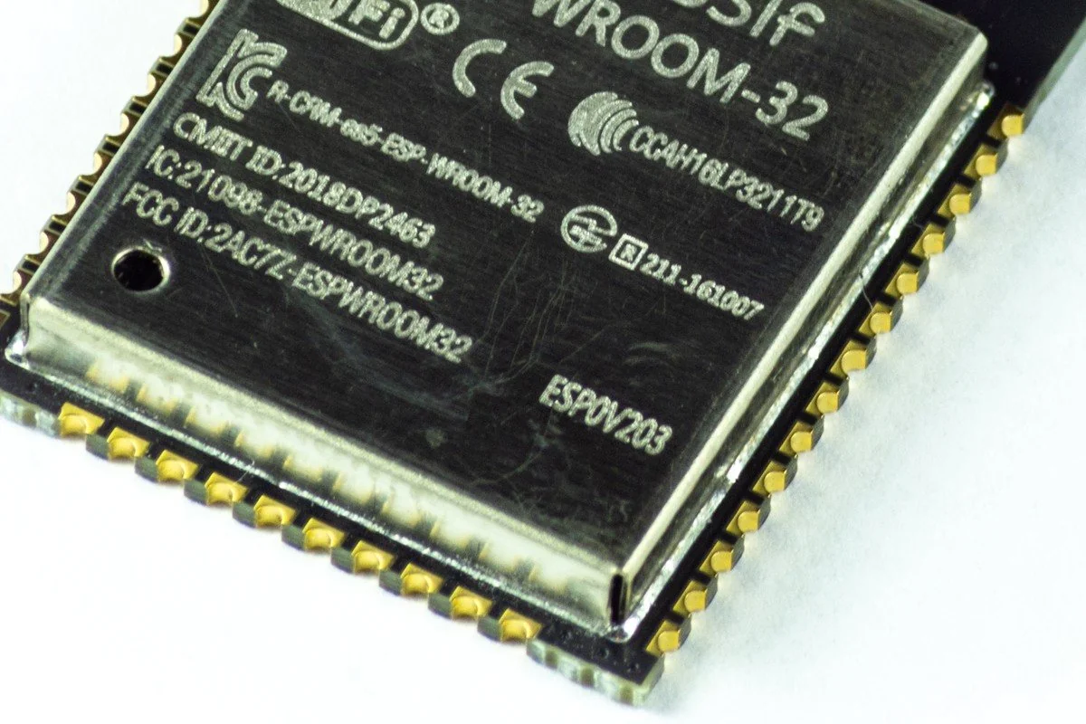
In commercial hardware development, profitability is decided at the schematic design table. A hardware product can deliver flawless technical performance in the laboratory, but if its Bill of Materials (BOM) cost exceeds target economic thresholds, the product will fail commercially in competitive B2B enterprise tenders.
Many engineering teams fall into the trap of "over-specifying" components: specifying 16-bit ADCs when 12-bit is sufficient, scattering 40 unique resistor values across a board, and selecting single-source proprietary ICs with 52-week factory lead times. Conversely, clumsy cost-cutting—such as substituting unvetted gray-market capacitors or dropping essential surge protection diodes—triggers devastating field warranty returns.
True Value Engineering (VE) cuts 20% to 40% of manufacturing unit cost through architectural intelligence: silicon platform consolidation, passive component rationalization, second-source footprint planning, and assembly DFM optimization.
This technical guide details DeviceLab's proven methodology for optimizing electronics BOM economics while maintaining uncompromising industrial reliability.
---
1. When to Optimize: The Rule of Cost Locking
The golden rule of hardware economics: 80% of final unit production cost is permanently locked before the first PCB trace is routed. Attempting to optimize a BOM after prototype validation only yields minor component discounts. Major cost breakthroughs require architectural decisions made at schematic inception: selecting the optimal silicon core, choosing between discrete vs. integrated power stages, and right-sizing memory density.
[ Architectural Phase (EVT) ] ──► Locks 80% of Unit Manufacturing Cost
             │
[ PCB Layout Phase (DVT) ]     ──► Locks 15% of Cost (Layer counts, enclosure dimensions)
             │
[ Procurement Phase (PVT) ]    ──► Negotiates final 5% (Distributor volume tier discounts)
---
2. Four High-Impact Strategies for Strategic BOM Reduction
1. Silicon Platforming & MCU Standardization
2. Passive Component Rationalization (Reel Consolidation)
3. Mandatory Second-Source Footprint Design
4. PCB Layer Count & Surface Area Optimization
1. Silicon Platforming Across Product Lines
Rather than choosing an STM32 for one product, an ESP32 for another, and an NXP core for a third, standardizing your entire hardware portfolio on a single MCU family pools enterprise purchase volumes, unlocking tier-1 pricing while software teams reuse 80% of their embedded driver codebase.
2. Passive Component Rationalization
An unoptimized board might incorporate 45 different resistor values. On an automated SMT assembly line, every unique part number requires loading a separate feeder reel, incurring setup fees and slowing down pick-and-place indexing. By standardizing on common values (10kΩ, 1kΩ, 100Ω) and 0.1µF/10µF capacitors, you reduce unique line items from 70 down to 25, dramatically slashing assembly costs.
3. Mandatory Second-Source Footprints
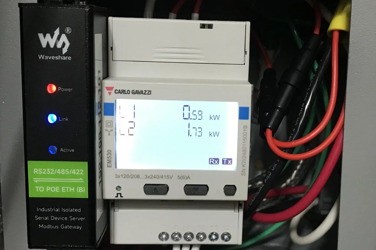
Every critical active component (LDO voltage regulators, RS485 transceivers, op-amps, Flash memory) must be assigned a secondary, pin-compatible alternative from a competing manufacturer. If one supplier experiences supply chain disruptions or arbitrarily raises prices, the manufacturing line seamlessly swaps in the second-source part without modifying the PCB layout.
4. PCB Layer Count & Board Area Rationalization
Careful component floorplanning and escape routing can frequently collapse an expensive 6-layer design into a tightly optimized 4-layer stackup, cutting bare board fabrication costs by 35% to 50%.
---
DeviceLab Value Engineering & BOM Optimization Services
DeviceLab provides comprehensive hardware cost-down redesign and procurement services:
- Comprehensive BOM Architecture Audits: Surgical review of client schematics, identifying over-specified silicon, single-source risks, and obsolete components.
- Form-Fit-Function Drop-In Redesigns: Updating PCB layouts to accommodate cost-effective second-source components while maintaining exact mechanical and electrical interchangeability.
- Factory Direct Procurement Power: Sourcing components directly through franchised tier-1 global distributors and regional manufacturers with guaranteed authenticity and competitive volume pricing.
Explore our related hardware design and manufacturing guides: