

Developing a commercial, B2B electronic hardware product is fundamentally different from building software applications or hobbyist breadboard experiments. In software development, bugs can be patched instantly with a hotfix. In hardware engineering, an unvetted silicon selection, inverted pinout, or broken ground plane necessitates physical PCB respins, delays production by months, and wastes tens of thousands of dollars in tooling and components.
To mitigate commercial risk, professional Original Design Manufacturers (ODMs) and electronics design houses enforce a disciplined, phased development lifecycle: progressing systematically through architectural definition, schematic simulation, multi-layer PCB layout, and the standardized EVT (Engineering Validation Test) -> DVT (Design Validation Test) -> PVT (Production Validation Test) validation gates.
This technical guide provides an exhaustive blueprint of the B2B electronic hardware design methodology practiced at DeviceLab.
---
1. The 6-Stage Hardware Development Lifecycle

[ Stage 1: Product Brief & Architecture ] ──► [ Stage 2: Schematic Capture & BOM Sourcing ]
                                                                  │
[ Stage 4: EVT Prototype Bring-Up ]       ◄── [ Stage 3: High-Speed PCB Layout & DFM ]
         │
[ Stage 5: DVT Validation & Pre-EMC ]     ──► [ Stage 6: PVT Pilot Run & Mass Manufacturing ]
Stage 1: Product Requirements & Technical System Architecture
Transform commercial business requirements into an unambiguous engineering specification: power budget analysis, microcontroller selection, communication protocol matrices, and environmental ratings.
Stage 2: Schematic Capture & Strategic Component Sourcing
Electrical engineers design schematic blocks in Altium Designer. Component selection emphasizes tier-1 manufacturers with guaranteed 10+ year production lifecycles, assigning secondary pin-compatible alternatives across all critical silicon.
Stage 3: Multi-Layer PCB Layout & Design for Manufacturing (DFM)
Layout engineers implement proper layer stackups, route controlled-impedance tracks, maintain continuous reference ground planes, and design thermal vias for high-current regulators.
Stage 4: Engineering Validation Testing (EVT)
First-spin prototype PCBAs are powered up under bench supplies. Hardware engineers probe clock oscillators, power rail ripple, and peripheral buses using high-bandwidth digital oscilloscopes.
Stage 5: Design Validation Testing (DVT)
Assembled boards inside final enclosures undergo thermal cycling (-20°C to +70°C), vibration stress tests, ESD air/contact discharges, and RF radiated emissions pre-compliance in an anechoic chamber.
Stage 6: Production Validation Testing (PVT) & Mass Production
The pilot manufacturing run evaluates mass assembly line yields. Automated test fixtures (pogo-pin ICT/FCT jigs) program firmware and log calibration metrics automatically.
---
2. Preventing Hardware Failures: The Joint HW/FW Design Review
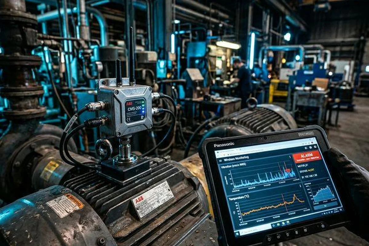
The single most frequent cause of prototype respins is disconnect between hardware engineers and firmware developers. DeviceLab enforces formal cross-reviews:
Hardware Schematics  <== Synchronous Cross-Review ==>  Embedded Firmware Drivers
- GPIO Multiplexing                                    - Interrupt Priorities
- Boot Strap Pin Defaults                              - DMA Channel Conflicts
- Power Rail Sequencing                                - Sleep Wakeup Triggers
- Verifying Boot Strap Pins: Ensuring pull-up/pull-down resistors on MCU strapping pins do not inadvertently lock the processor into bootloader flashing modes during normal startup.
- Validating Peripheral Mapping: Confirming that high-speed communication peripherals (SPI, I2C, UART) do not conflict with timer capture channels or dedicated hardware interrupt lines.
---
DeviceLab Turn-Key Hardware Engineering Capabilities
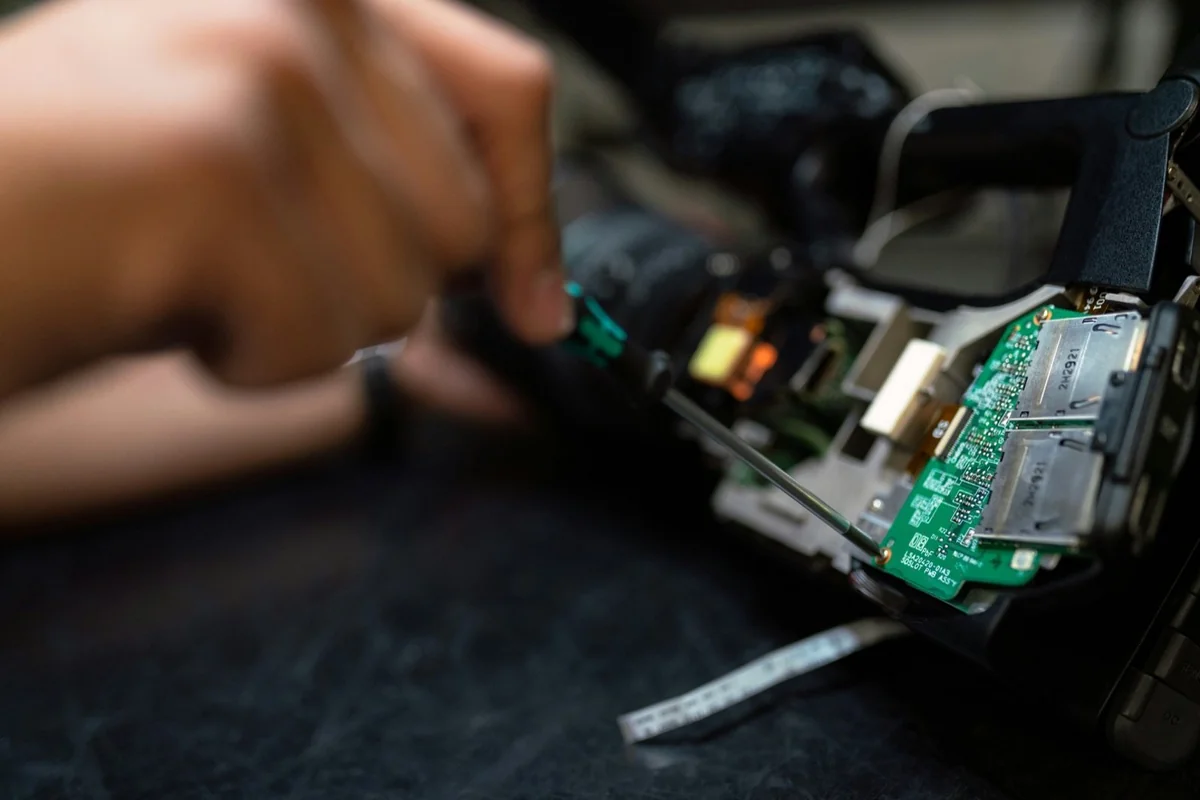
DeviceLab acts as your dedicated electronic hardware R&D department:
- Architecture to Mass Production: Comprehensive ownership of electronic schematics, multi-layer PCB layout, embedded firmware, mechanical CAD, and supply chain logistics.
- Turnkey Hardware & Technical Documentation: Fully tested hardware units, complete wiring pinout guides, technical datasheets, and manufacturer warranty support upon project completion.
- Production-Ready Engineering: Eliminating expensive design respins through upfront DFM, DFT, and regulatory pre-compliance testing.
Explore related technical guides: