

Do you already have a verified electrical schematic and merely require professional PCB layout routing, or do you have a functional product requirement that must be engineered from concept to market? Both scopes are frequently lumped under the broad umbrella of "circuit design," yet they represent vastly different technical workflows, timelines, and engineering deliverables.
Misjudging this boundary leads to project misalignments: hiring a pure layout draftsman when you actually need architectural circuit simulation and firmware development, or conversely, paying for full system R&D when your electrical schematics are already 100% frozen.
This guide clarifies how to identify your current project stage, evaluate the required technical scope, and choose the most cost-effective engineering path.
---
1. Comparing PCB Layout vs. Full Electronic Device R&D

[ Pure PCB Layout Scope ]
Schematic & Netlist (Client Supplied) ──► Placement & Routing ──► Manufacturing Gerbers

[ Full Device R&D Scope ]
Product Brief ──► Architecture ──► Schematics ──► PCB Layout ──► Firmware ──► Prototypes ──► Mass Production
- PCB Layout: The physical implementation of an electrical circuit. The layout engineer places components on board layers, routes copper tracks adhering to design rules (clearances, trace widths, differential impedance), optimizes thermal dissipation, and outputs fabrication deliverables (Gerber RS-274X/ODB++, drill files, pick-and-place XY data).
- Full Device R&D: The comprehensive electronic product development lifecycle. It begins with operational specifications and encompasses silicon MCU selection, power supply architecture, analog sensor conditioning, schematic capture, multi-layer layout, embedded C/C++ firmware development, mechanical 3D CAD modeling, lab bring-up, and certification pre-testing.
---
2. When Standalone PCB Layout Services Are Sufficient
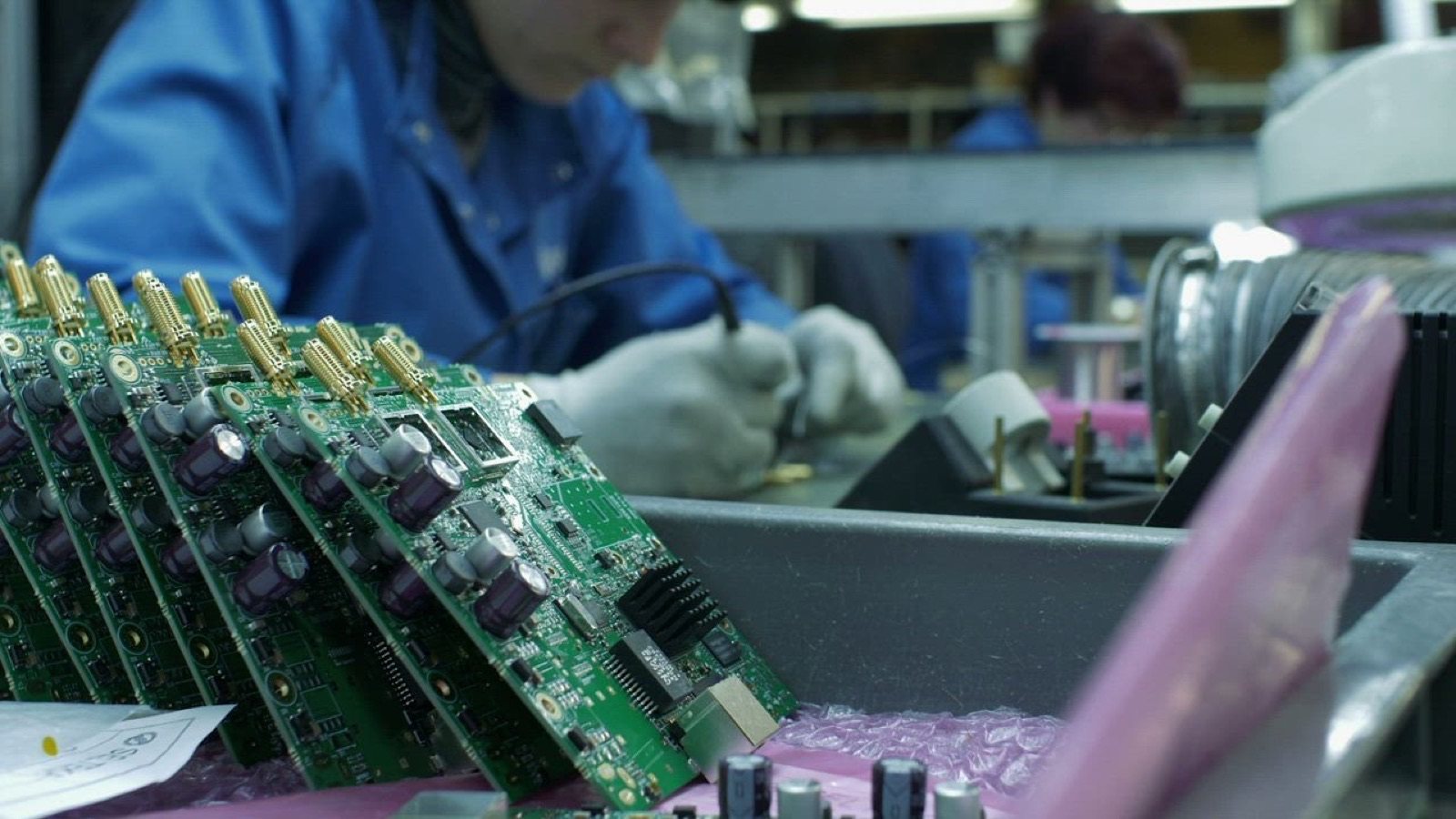
Standalone PCB layout is the optimal, cost-efficient choice when your team's electrical design is already validated:
- Schematics & Netlist are Frozen: You possess a complete schematic capture in Altium Designer, KiCad, or OrCAD with zero unresolved electrical floating nets.
- Core Components & BOM are Selected: Key silicon (MCUs, transceivers, DC-DC regulators) is finalized with vetted manufacturer part numbers.
- Mechanical Form Factor is Defined: Board outline, mounting hole locations, connector keep-out zones, and maximum component height limits are documented.
- Stackup & Routing Rules are Specified: Target impedance requirements (e.g., 50Ω single-ended, 90Ω USB, 100Ω Ethernet differential pairs) are established.
---
3. When Full Device R&D Engineering is Mandatory

Enterprises require end-to-end device development when the starting point is an operational concept or functional requirement:
System Architecture -> Component Sourcing -> Schematic Capture -> PCB Layout -> Firmware -> Pilot Run
1. Functional Brief Stage
You have a product vision—such as an industrial battery-powered vibration sensor or an IoT agricultural controller—but have not determined the processor silicon, power rail topologies, or RF matching components.
2. Multi-Disciplinary Hardware & Firmware Interdependence
Hardware performance cannot be evaluated in isolation from firmware: power consumption depends on microcontroller sleep states, while peripheral timing (SPI, I2C, DMA) requires co-design between hardware registers and firmware drivers.
3. Industrial Regulatory & EMC Compliance
Commercial deployment requires meeting rigorous electromagnetic compatibility standards (FCC Part 15, CE RED, CISPR 32). Achieving compliance demands front-end circuit filtering, continuous ground return plane design, and transient TVS suppression engineered into the schematic before the first PCB trace is routed.
---
DeviceLab Hardware Engineering Services

DeviceLab provides flexible engagement models matching your project maturity:
- Standalone High-Speed PCB Layout: Rapid layout services delivering IPC-compliant multi-layer designs, controlled impedance routing, and optimized DFM/DFT packages.
- Turn-Key Electronic Device R&D: Complete hardware and firmware product development—from initial architecture and prototype fabrication to volume SMT manufacturing.
- Hardware Architecture Audits: Design reviews of existing schematics and PCB layouts to resolve thermal hotspots, signal integrity reflections, and EMC test failures.
Related technical resources: