
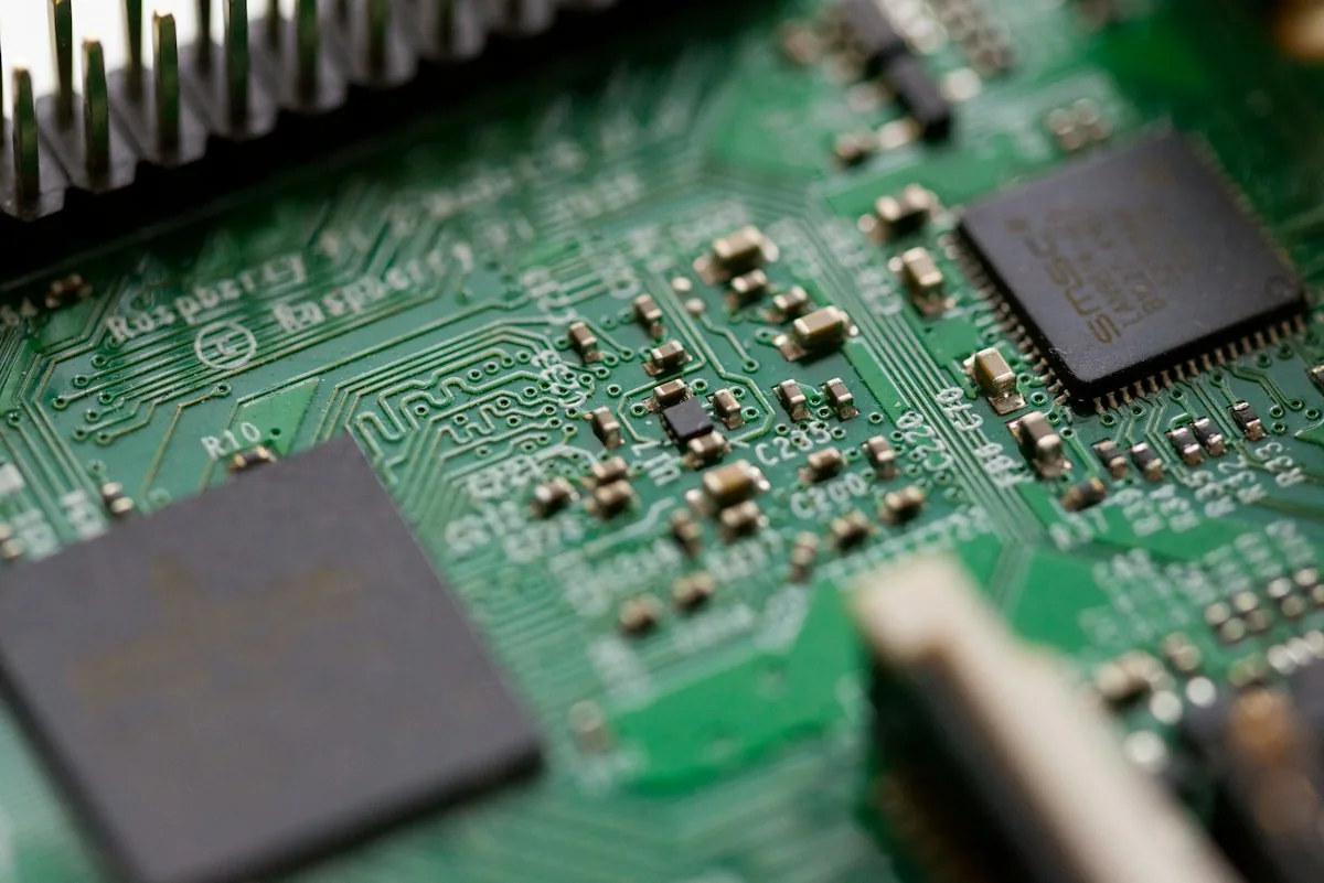
Transforming electronic CAD designs into physical, functional hardware requires a coordinated manufacturing pipeline: raw printed circuit board fabrication, global component procurement, high-precision Surface Mount Technology (SMT) soldering, and rigorous quality inspection. For commercial enterprises, managing multiple fragmented vendors—a PCB fab house, multiple component distributors, an assembly factory, and a test lab—introduces compounding logistical friction, component obsolescence delays, and finger-pointing when defects arise.
Turnkey PCBA manufacturing consolidates the entire hardware physicalization process under a single responsible engineering umbrella: from Gerber Design for Manufacturing (DFM) verification to component sourcing, automated assembly, X-ray inspection, and final functional flashing.
This comprehensive technical guide outlines the end-to-end PCBA manufacturing lifecycle: raw board fabrication parameters, SMT assembly mechanics, automated quality assurance workflows, and strategies for scaling from 10 pilot prototypes to tens of thousands of production units.
---
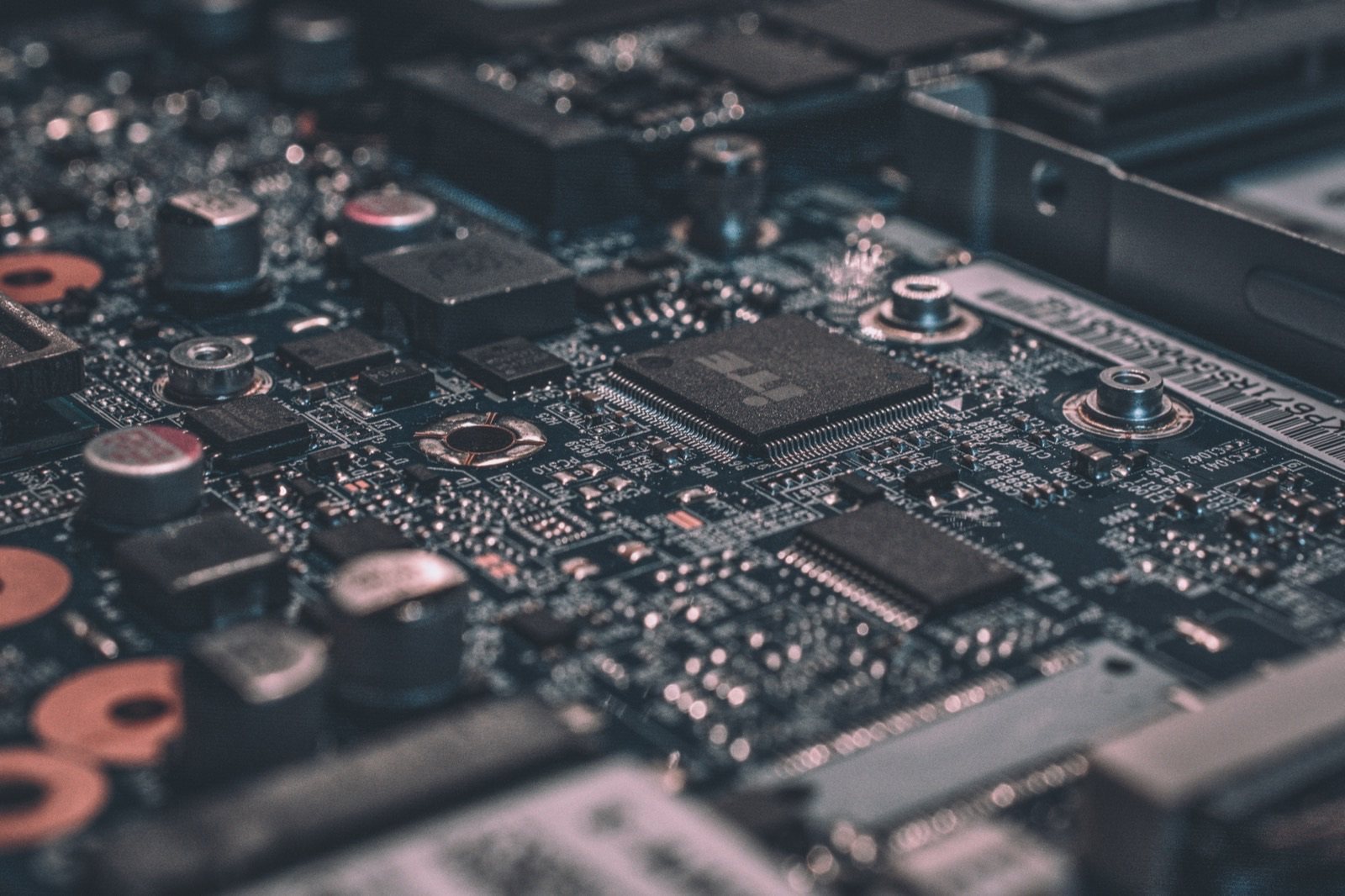
1. Bare PCB Board Fabrication Technologies
[ FR-4 / High-Tg Core ] ──► [ Copper Foil Etching ] ──► [ Multi-Layer Lamination ]
                                                                ↓
[ Surface Finish: ENIG / HASL ] ◄── [ Solder Mask / Silkscreen ] ◄── [ CNC Drilling & Plating ]
Critical Fabrication Parameters:
- Dielectric Substrates: Standard FR-4, High-Tg FR-4 for lead-free reflow, and Rogers/PTFE high-frequency laminates for RF microwave antennas.
- Surface Finishes: Electroless Nickel Immersion Gold (ENIG) is the gold standard for fine-pitch BGA and QFN packages, providing a planar surface that prevents oxidation and withstands multiple thermal reflow cycles. Hot Air Solder Leveling (HASL) remains an economical choice for simple through-hole designs.
- Controlled Impedance Tolerances: Standard fabrication holds ±10% impedance tolerance; precision RF and high-speed memory traces achieve ±5% through coupon TDR testing.
---
2. The Precision SMT Assembly Manufacturing Pipeline
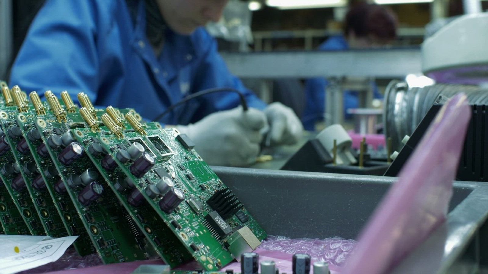
Automated Surface Mount Technology (SMT) executes across five automated sequential stations:
1. Solder Paste Printing ──► 2. 3D SPI ──► 3. High-Speed Pick-and-Place
                                                    ↓
5. 3D AOI & X-Ray Testing ◄── 4. Reflow Soldering (10-Zone Profile)- Precision Stencil Printing: Laser-cut stainless steel stencils deposit lead-free solder paste (SAC305) onto PCB surface pads with sub-mil thickness accuracy.
- 3D Solder Paste Inspection (SPI): Optical scanners measure solder deposit height, volume, and alignment. Catching printing defects at this stage eliminates over 70% of potential soldering faults before components are placed.
- High-Speed Pick-and-Place: Precision automated mounters position miniature 0201/0402 passives at rates exceeding 40,000 components per hour, while vision-guided fine-pitch placers mount large multi-ball BGAs and QFPs with micron-level alignment.
- Multi-Zone Convection Reflow Soldering: Boards traverse a 10-zone reflow oven following a strictly controlled thermal profile to guarantee optimal intermetallic grain structure without thermal shock.
- 3D Automated Optical Inspection (AOI) & 2D/3D X-Ray: AOI cameras verify component presence, polarity orientation, solder fillets, and tombstoning. Deep X-ray inspection penetrates BGA packages to confirm void-free solder balls and zero micro-bridging.
---
3. Comprehensive Quality Verification & Functional Testing (FCT)
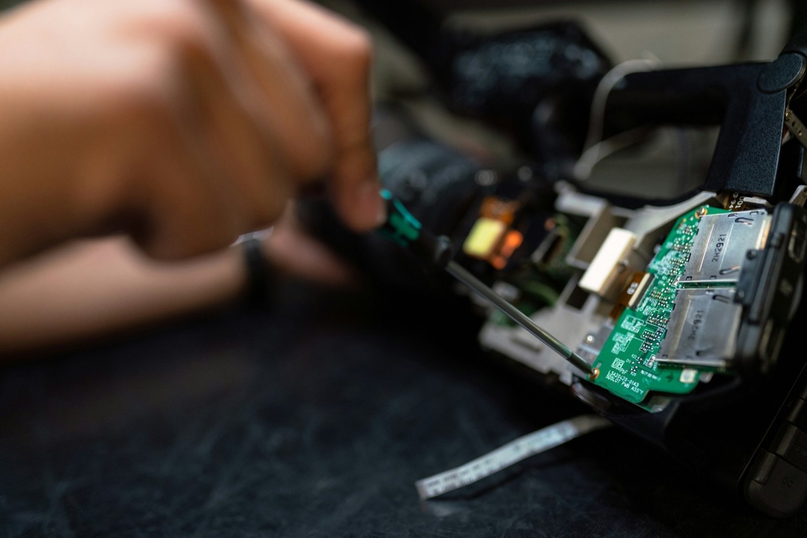
A visually pristine circuit board is not guaranteed to function electrically. Production runs must undergo progressive electrical verification:
[ Automated Optical (AOI) ] ──► [ In-Circuit Testing (ICT) ] ──► [ Functional Testing (FCT) ]
- In-Circuit Testing (ICT): Custom "bed-of-nails" test fixtures press spring-loaded pogo pins against designated PCBA test pads to verify resistance, capacitance, diode junctions, and check for power-to-ground shorts before power is applied.
- Functional Circuit Testing (FCT): The board is placed into a custom automated test jig that connects to power supplies, injects simulated sensor signals, flashes firmware binaries via SWD/JTAG, and verifies communication responses across RS485, CAN, Wi-Fi, and cellular interfaces.
---
DeviceLab Turnkey PCBA Services
DeviceLab provides comprehensive PCB manufacturing and electronic box-build services:
- Rapid Prototyping (2 to 4 Days): Fast-turn PCB fabrication and assembly for engineering verification tests (EVT) and design validation tests (DVT).
- Component Lifecycle Management: Sourcing exclusively through authorized franchised distributors with guaranteed authenticity certificates and second-source BOM planning.
- Turnkey Box-Build Integration: Complete mechanical assembly, wire harnessing, conformal coating, custom injection-molded plastic enclosures, and retail packaging.
Explore our related manufacturing and engineering capabilities: