

In high-speed digital and precision mixed-signal electronics, a printed circuit board is not merely a passive wiring harness connecting components; it is an active, distributed-element transmission network. As clock frequencies rise and edge rates sharpen into the sub-nanosecond domain, improper trace routing, broken ground return paths, or inadequate power decoupling transform ordinary circuit traces into transmission lines prone to severe signal integrity (SI) reflections, electromagnetic emissions (EMI), and cross-talk interference.
Transitioning from hobbyist two-layer boards to commercial-grade multi-layer PCBAs requires strict adherence to high-frequency physics, rigorous thermal dissipation rules, and Design for Manufacturing (DFM) tolerances.
This technical guide details advanced PCB layout methodologies: continuous ground plane management, controlled impedance routing, decoupling loop inductance minimization, and DFM guidelines that prevent costly factory assembly rework.
---
1. High-Speed Return Current Paths & Ground Plane Integrity

A fundamental rule of high-speed PCB engineering: Current flows in closed loops.
Low-Frequency DC:     Current follows path of least RESISTANCE (Spreads widely across copper)
High-Frequency AC:    Current follows path of least INDUCTANCE (Directly underneath the trace)
CORRECT: Signal Trace over Continuous Solid Ground Plane
Signal Trace Layer:    ────────────────────────────────────────
Dielectric Core:
Solid Ground Layer:    ========================================
                       (Return current mirrors signal directly underneath)

FATAL ERROR: Signal Trace Crossing a Split or Slot in Ground Plane
Signal Trace Layer:    ───────────────────┬────────────────────
Dielectric Core:                          │
Split Ground Layer:    =========== [ SPLIT GAP ] ==============
                                          └─► Detour creates massive EMI loop!
The Peril of Ground Plane Splits
When a high-speed digital trace (SPI clock, USB data, MCU bus) crosses a slit, moat, or void in the underlying reference plane, the return current cannot follow its natural path directly beneath the conductor. It is forced to take a wide detour around the gap. This detour creates a high-inductance current loop that functions as a loop antenna, generating radiated electromagnetic interference (EMI) and causing ground bounce.
---
2. Decoupling Capacitor Placement & Parasitic Inductance Minimization
Decoupling capacitors serve as local energy reservoirs, supplying transient switching currents to digital ICs during logic transitions. If capacitor placement introduces parasitic trace inductance, the capacitor cannot react quickly enough, causing supply rail sag and logic errors.
Optimal Decoupling Loop:
Power Plane Via ──► Capacitor Pad ──► IC Power Pin
                        │
Ground Plane Via ◄── Capacitor GND Pad- Physical Proximity: Mount decoupling capacitors (0.1µF / 1µF 0402 ceramic MLCCs) on the same layer as the IC, directly abutting the power pins.
- Minimize Via Inductance: Place ground and power vias immediately beside the capacitor surface-mount pads using wide traces. Never route thin, winding traces between a decoupling capacitor and an IC pin.
- Dedicated Pin Decoupling: Every single power pin on an MCU or FPGA must possess its own dedicated decoupling capacitor; never force multiple power pins to share a single capacitor.
---
3. Signal Integrity & Controlled Impedance Routing
| High-Speed Interface | Routing Topology | Differential Impedance | Single-Ended |
|---|---|---|---|
| USB 2.0 (High Speed) | Tightly coupled differential pair | 90Ω ± 10% | 45Ω |
| Ethernet (100/1000Base-T) | Symmetrical differential pair | 100Ω ± 10% | 50Ω |
| RS485 Industrial Bus | Differential pair, guarded | 120Ω ± 10% | 60Ω |
| RF Antenna Feeds (Wi-Fi/BLE) | Coplanar waveguide with ground | N/A | 50Ω ± 5% |
- Enforce Length Matching: Ensure positive and negative differential legs match in physical length within tight tolerances (±0.15mm for USB and Ethernet) to eliminate phase skew.
- The 3W Crosstalk Mitigation Rule: Maintain a spacing of at least 3× the trace width between adjacent high-speed signal lines to reduce mutual inductive coupling by 70%.
---
4. Design for Manufacturing (DFM) & Assembly (DFA) Standards
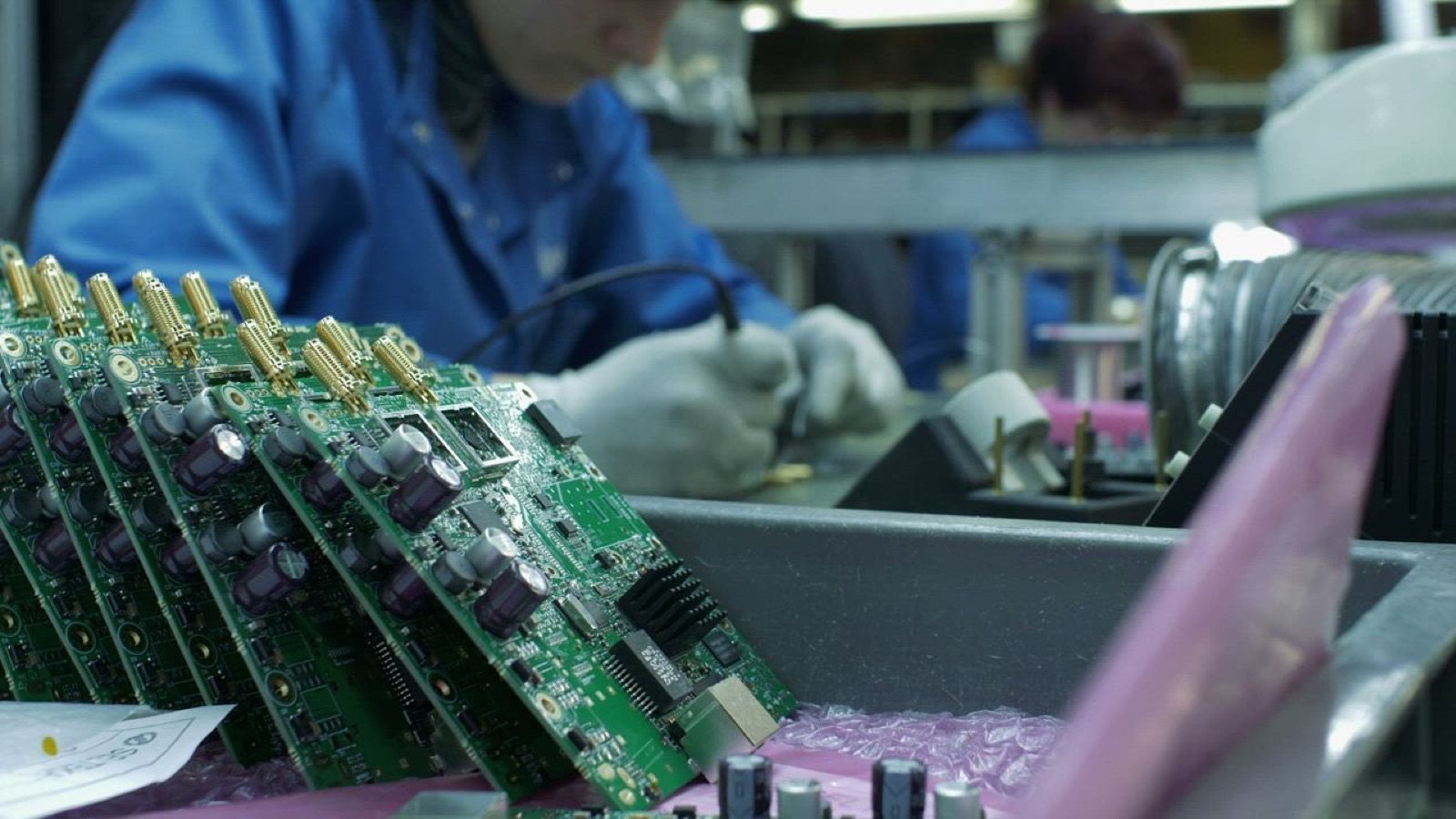
A layout that functions on a simulation screen can still cause devastating yield losses during automated Surface Mount Technology (SMT) assembly:
- Avoid Acid Traps: Never route traces meeting at acute angles. Acute corners trap chemical etching acid during fabrication, over-etching copper and causing hairline open circuits.
- Tombstoning Prevention: On passive components (0402, 0603 resistors and capacitors), balance the copper thermal mass of both pads. If one pad connects to a massive ground plane while the other connects to a thin trace, the thin pad melts first during reflow soldering, pulling the component upright. Always use thermal relief cross-spokes on plane connections.
- Fiducial Markers: Place three non-symmetrical 1.0mm circular copper fiducial marks on surface layers to allow automated SMT pick-and-place optical cameras to achieve sub-micron component alignment.
---
DeviceLab Advanced Layout Capabilities
DeviceLab delivers world-class layout engineering for demanding high-reliability applications:
- Complex Multi-Layer Layouts: 4-layer to 16-layer stackups engineered with blind, buried, and micro-vias for high-density BGA packages.
- RF & Microwave Routing: 50Ω coplanar waveguides with via fences, striplines, and antenna tuning for 2.4GHz, 5.8GHz, and Sub-1GHz bands.
- Full DFM/DFA Verification: Pre-fabrication Gerber rule checks guaranteeing >99.5% first-pass SMT assembly yields.
Explore our related hardware engineering guides: