
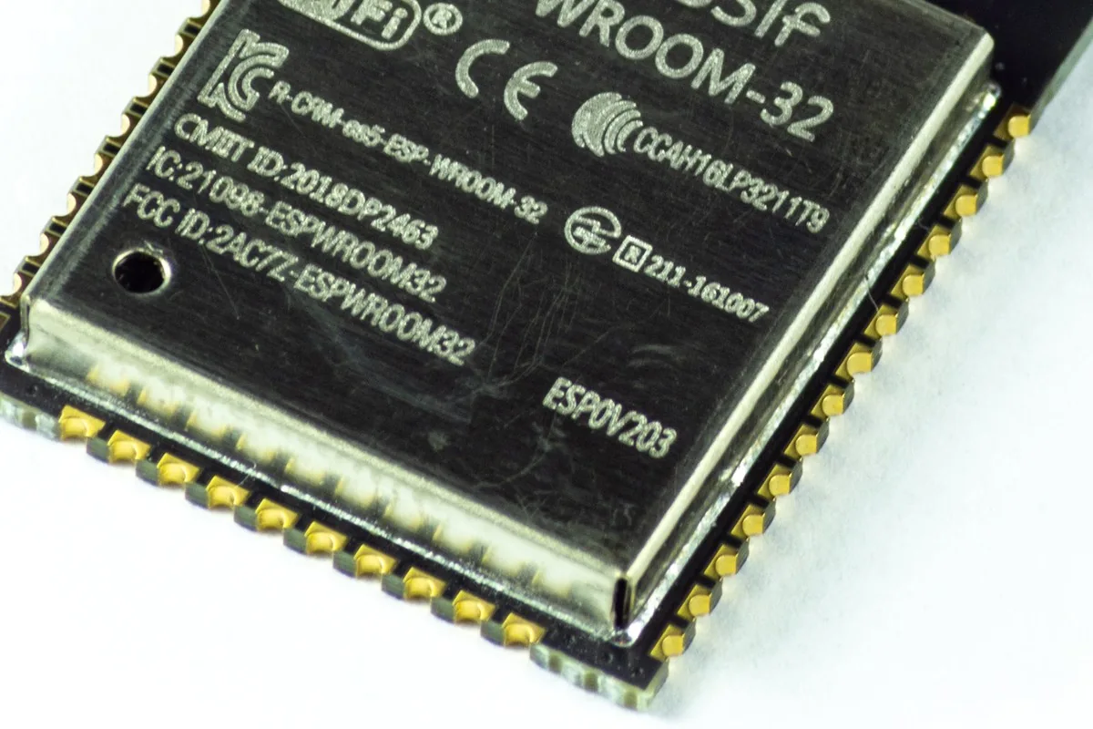
Commercial IoT modules—spanning cellular 4G LTE-M/NB-IoT, LoRaWAN, Wi-Fi 6, and Bluetooth Low Energy—have revolutionized rapid hardware prototyping. Pre-certified surface-mount modules allow engineering teams to stand up connected Proof-of-Concept (PoC) demonstrators in weeks without designing complex multi-gigahertz RF matching circuits from scratch.
However, as a connected hardware initiative transitions from initial lab testing toward high-volume commercial production, relying on ad-hoc carrier boards and hobbyist dev kits becomes a critical liability. Loose jumper wires, lack of industrial surge suppression, unoptimized quiescent current draw, and fragile mechanical headers cause catastrophic field failure rates in harsh industrial environments.
This guide explores the engineering lifecycle of IoT modules: the strategic advantages of modular vs. chip-down RF design, the triggers that necessitate custom baseboard engineering, and DeviceLab's methodology for taking connected modules into mass production.
---
1. Modular RF Design vs. Chip-Down Design

A primary architectural decision in connected device development is choosing between pre-packaged RF modules and discrete "chip-down" implementations:
Pre-Certified Module: [ SoC + Crystals + RF Filter + Shielding Can ] -> Pre-Certified CE/FCC
                                      VS
Chip-Down Design: [ Bare Silicon IC + 50Ω Microstrip Trace + Matching Network + Custom Testing ]| Decision Factor | Pre-Certified IoT Module | Discrete Chip-Down Design |
|---|---|---|
| RF Compliance Testing | Inherits module modular FCC/CE/RED grant | Full standalone radio certification ($30,000 – $80,000+) |
| RF Engineering Complexity | Low (50Ω trace or onboard chip/U.FL antenna) | High (requires VNA impedance tuning, 4-layer RF stackup) |
| Unit BOM Cost | Moderate ($4.00 – $18.00 depending on cellular/Wi-Fi) | Lowest ($1.20 – $5.00 for bare silicon) |
| Production Volume Threshold | Optimal from 100 to 50,000 units/year | Only economically justifiable at >100,000 units/year |
| Time to Market | 2 to 4 months | 9 to 15 months |
For 95% of industrial B2B devices, using pre-certified modules soldered onto a custom-engineered motherboard is the gold standard approach: it captures 80% of BOM savings while completely sidestepping RF certification and antenna redesign risks.
---
2. When Does an Enterprise Need a Custom Baseboard for IoT Modules?
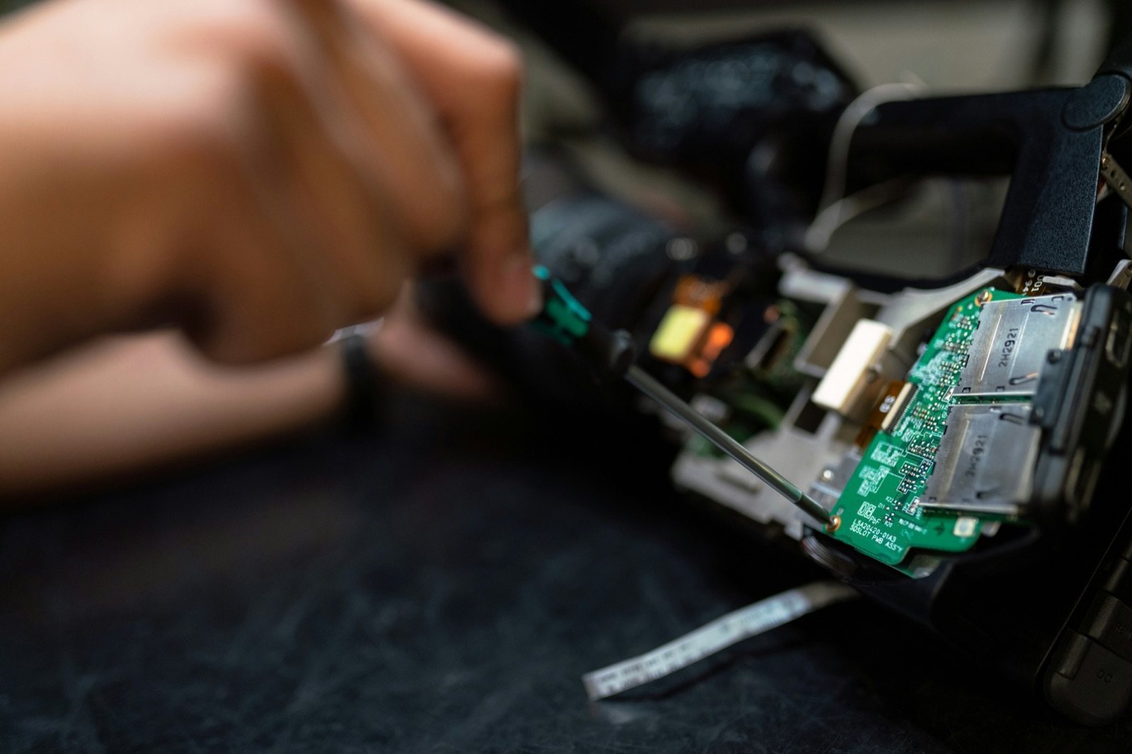
While the core wireless module can be sourced off-the-shelf, the surrounding electronics must be custom-engineered for industrial survivability:
[ Pre-Certified Wireless Module (Cellular / LoRa / BLE) ]
                          │
   ┌──────────────────────┴──────────────────────┐
   │ Custom Industrial Carrier PCBA (DeviceLab)  │
   │ ├── 9-36VDC Wide-Input Buck Converter       │
   │ ├── 8kV/15kV ESD Protection & TVS Diodes    │
   │ ├── Galvanically Isolated RS485 / CAN Port  │
   │ ├── Precision Analog Front-End (4-20mA)     │
   │ └── Ultra-Low-Leakage Sleep Power Gating    │
   └─────────────────────────────────────────────┘
1. Power Supply Stability & Surge Suppression
Industrial electrical panels deliver noisy 24VDC power polluted by inductive flyback spikes from heavy contactors and solenoids. Standard dev boards powered by 5V micro-USB will instantly blow up. A custom baseboard incorporates wide 9–36VDC input buck converters, polarity reversal diodes, and primary Gas Discharge Tubes (GDT) / TVS clamps capable of surviving EN 61000-4-5 surge testing.
2. Tailored Field Sensor Interfaces
Generic development kits provide 0.1-inch male header pins that vibrate loose on machinery. A custom board terminates field signals through rugged pluggable screw terminals or spring-cage blocks, hosting dedicated signal conditioning circuitry for 4–20mA current loops, 0–10V analog transducers, and dry-contact pulse inputs.
3. Battery Life Optimization for Edge Nodes
Off-the-shelf development boards feature power-hungry linear dropout (LDO) regulators, always-on status LEDs, and USB-UART bridge chips that continuously bleed 10mA to 30mA of quiescent current. In contrast, a custom-designed low-power IoT node incorporates high-efficiency micropower buck regulators and MOSFET power gates that cut deep sleep standby current down to under 15 microamps, extending battery life to 5–10 years on lithium thionyl chloride (Li-SOCl2) cells.
---
DeviceLab Module Integration & PCBA Capabilities
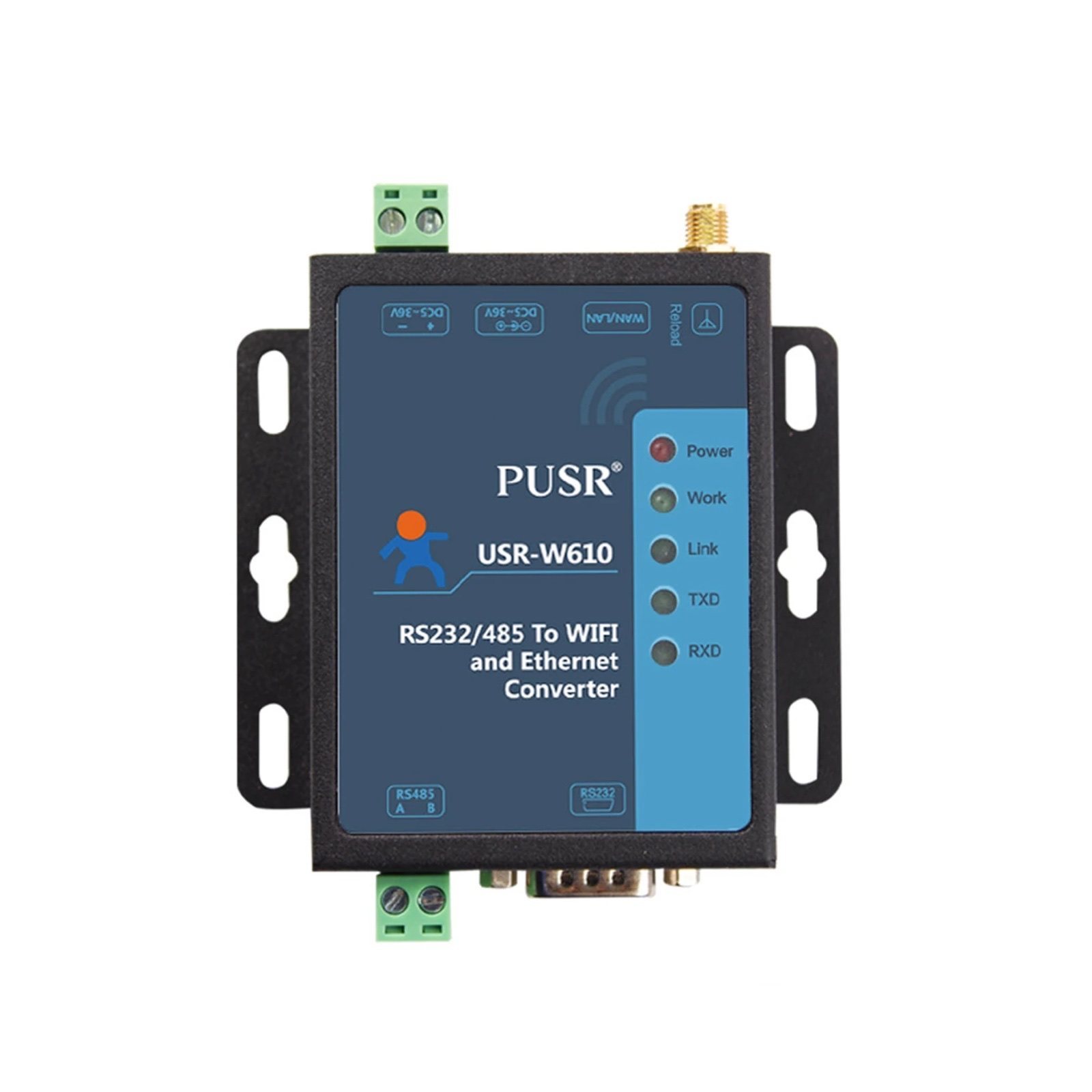
DeviceLab partners with hardware innovators to turn wireless modules into rugged commercial products:
- RF Carrier PCBA Design: 4-layer and 6-layer PCB stackups engineered with controlled 50Ω coplanar waveguides, ground stitching vias, and certified trace antennas.
- Embedded Firmware & Low-Power Scheduling: Deterministic FreeRTOS and bare-metal firmware implementing periodic wake-up cycles, eDRX/PSM cellular scheduling, and local flash buffering.
- Complete Box-Build & In-Circuit Testing: Precision SMT placement, automated optical inspection (AOI), conformal silicone coating for moisture/dust protection, and custom DIN-rail or IP67 enclosure integration.
Related technical guides and capabilities: