

Developing a commercial, production-ready IoT device is a multi-disciplinary engineering endeavor spanning electrical schematic design, multi-layer high-speed PCB layout, low-level embedded firmware, industrial RF compliance, and scalable mass manufacturing. While software proofs-of-concept can be spun up in days using cloud templates and hobbyist dev kits, delivering physical hardware that operates autonomously for years in remote field environments without lockups or power brownouts requires rigorous engineering discipline.
Many enterprise IoT initiatives fail when moving from laboratory prototypes to market launch due to unexpected electromagnetic compatibility (EMC) failures, battery drain oversights, thermal throttling, or component obsolescence.
This guide provides a comprehensive roadmap for enterprise hardware development: architectural foundations, critical failure modes to avoid, and DeviceLab's proven 6-stage productization methodology.
---
1. The Anatomy of an Enterprise-Grade IoT Device
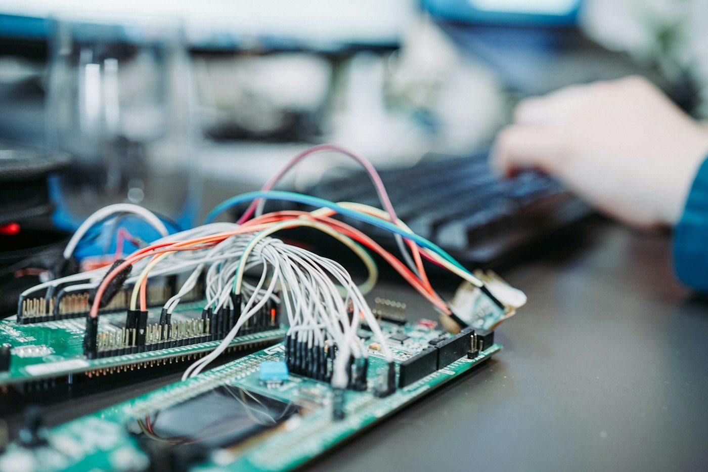
An industrial or commercial IoT device consists of four tightly synchronized subsystems:
+------------------------------------------------------------------------+
| 1. CORE PROCESSING & MEMORY SUBSYSTEM                                  |
| 32-bit ARM Cortex-M/A MCU/SoC, Secure Element (Atecc608), Flash Storage|
+------------------------------------------------------------------------+
| 2. ANALOG & SENSOR FRONT-END                                           |
| 4-20mA, 0-10V, RS485 Isolated Transceiver, I2C/SPI Sensor Conditioning |
+------------------------------------------------------------------------+
| 3. SECURE WIRELESS & TELEMETRY SUBSYSTEM                               |
| 4G LTE-M / NB-IoT / LoRaWAN / Wi-Fi 6, 50Ω Matched Antenna Array       |
+------------------------------------------------------------------------+
| 4. INDUSTRIAL POWER & SURGE PROTECTION STAGE                           |
| 9-36V Wide-Input Buck, TVS Diodes, GDT Clamps, Micro-Amp Sleep Gating  |
+------------------------------------------------------------------------+
- Power Management: Wide DC input regulators capable of absorbing 1kV–2kV electrical transients, coupled with ultra-low quiescent current sleep gating for battery-powered nodes.
- Deterministic Processing: ARM Cortex-M microcontrollers executing real-time operating systems (FreeRTOS) with independent hardware watchdogs.
- Sensor Front-End: High-precision ADCs, galvanically isolated fieldbus transceivers, and optical isolation barriers that prevent high-voltage machine noise from destroying digital silicon.
- RF Connectivity: Pre-certified wireless modules paired with precisely tuned impedance-matched trace or external antennas to maximize over-the-air link budgets.
---
2. The 6-Stage Engineering Lifecycle at DeviceLab
[ Phase 1: Architecture & Feasibility ] -> [ Phase 2: Schematic & BOM Optimization ]
                                                             ↓
[ Phase 4: Firmware & Security ]        <- [ Phase 3: High-Speed PCB Layout & DFM ]
       ↓
[ Phase 5: Prototype Bring-Up & Pre-EMC ] -> [ Phase 6: Pilot Run & Mass Manufacturing ]
Stage 1: Technical Architecture & Feasibility Analysis
We translate operational business briefs into rigorous technical specifications: power budget calculations, communication link budgets, thermal constraints, operating temperature ranges, and target BOM cost thresholds.
Stage 2: Schematic Design & Strategic Component Sourcing
Engineers design schematic circuits in Altium Designer, selecting tier-1 electronic components with guaranteed 10+ year availability lifecycles. Critical components (MCUs, transceivers, power ICs) are verified for multi-source pin-compatible alternatives to safeguard against supply chain disruptions.
Stage 3: Multi-Layer PCB Layout & Design for Manufacturing (DFM)
Layout engineers implement proper ground plane return paths, isolate noisy switching power supplies from sensitive RF traces, enforce 50Ω controlled impedance microstrips, and place automated in-circuit test (ICT) pogo-pin test pads across all critical nets.
Stage 4: Low-Level Firmware Development & Board Support Package (BSP)
Firmware engineers write production-grade C/C++ drivers, initialize hardware abstraction layers (HAL), implement robust state machines, and configure secure bootloaders with dual-bank fail-safe rollback Over-the-Air (OTA) update engines.
Stage 5: Prototype Bring-Up & Laboratory Pre-Compliance Testing
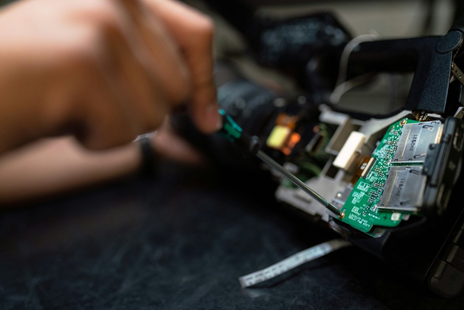
Bare PCBAs are assembled and tested under high-bandwidth digital oscilloscopes. Units undergo thermal imaging under maximum electrical load, ESD gun discharge testing (EN 61000-4-2), and pre-compliance spectrum analyzer sweeps to ensure pass rates at official certification labs.
Stage 6: Tooling, Pilot Run & Mass Manufacturing
DeviceLab coordinates automated SMT pick-and-place assembly, custom injection mold tooling for enclosures, automated functional test fixture development, and final packaging for commercial deployment.
---
DeviceLab Custom Device Design Capabilities
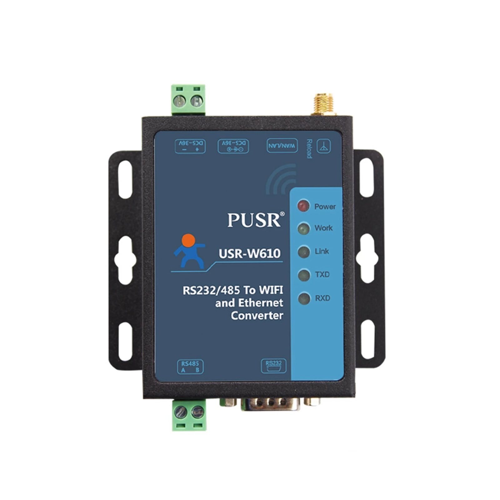
DeviceLab acts as a dedicated ODM/OEM engineering partner for enterprise hardware:
- Turn-Key Hardware & Firmware Co-Design: Complete ownership of electronic architecture, PCB layout, firmware stacks, and cloud integration.
- Intellectual Property Guarantee: 100% of all design files, Gerber data, BOMs, and source code transfer directly to the client enterprise.
- Rigorous DFM Standards: Ensuring seamless scalability from 50 prototype units to 50,000 production units with zero manufacturing surprises.
Explore our engineering services: